Rainbow Electronics MAX9938 User Manual
Page 2
MAX9938
1µA, 4-Bump UCSP/SOT23,
Precision Current-Sense Amplifier
2
_______________________________________________________________________________________
ABSOLUTE MAXIMUM RATINGS
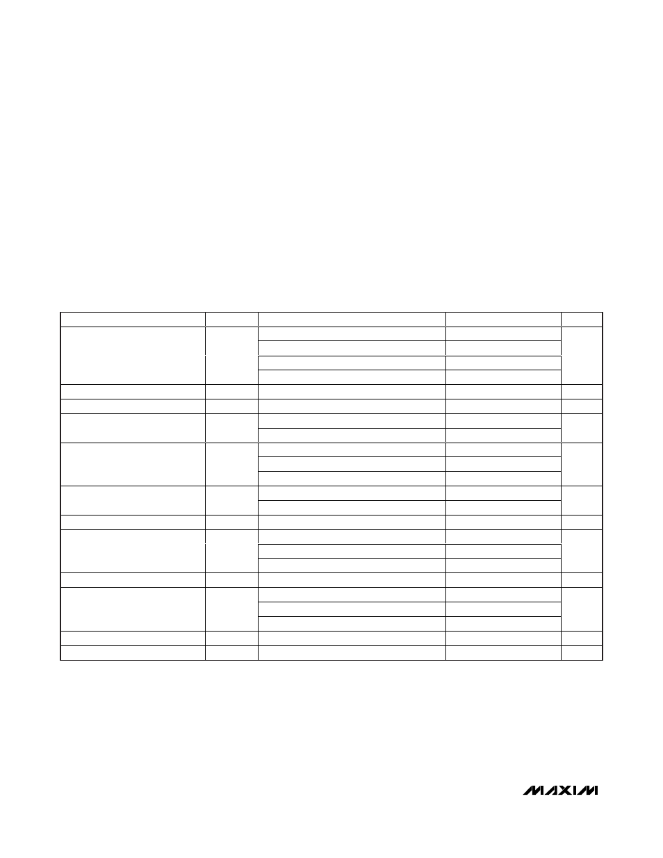
ELECTRICAL CHARACTERISTICS
(V
RS+
= V
RS-
= 3.6V, V
SENSE
= (V
RS+
- V
RS-
) = 0V, T
A
= -40°C to +85°C, unless otherwise noted. Typical values are at T
A
= +25°C.) (Note 1)
Stresses beyond those listed under “Absolute Maximum Ratings” may cause permanent damage to the device. These are stress ratings only, and functional
operation of the device at these or any other conditions beyond those indicated in the operational sections of the specifications is not implied. Exposure to
absolute maximum rating conditions for extended periods may affect device reliability.
Note 1: All devices are 100% production tested at T
A
= +25°C. All temperature limits are guaranteed by design.
Note 2: V
OUT
= 0. I
CC
is the total current into RS+ plus RS- pins.
Note 3: V
OS
is extrapolated from measurements for the gain-error test.
Note 4: Gain error is calculated by applying two values of V
SENSE
and calculating the error of the slope vs. the ideal:
Gain = 25, V
SENSE
is 20mV and 120mV.
Gain = 50, V
SENSE
is 10mV and 60mV.
Gain = 100, V
SENSE
is 5mV and 30mV.
Note 5: The device is stable for any external capacitance value.
Note 6: V
OH
is the voltage from V
RS-
to V
OUT
with V
SENSE
= 3.6V/gain.
PARAMETER
SYMBOL
CONDITIONS
MIN
TYP
MAX
UNITS
V
RS+
= 5V, T
A
= +25°C
0.5
0.85
V
RS+
= 5V, -40°C < T
A
< +85°C
1.1
V
RS+
= 28V, T
A
= +25°C
1.1
1.8
Supply Current (Note 2)
I
CC
V
RS+
= 28V, -40°C < T
A
< +85°C
2.5
μA
Common-Mode Input Range
V
CM
Guaranteed by CMRR , -40°C < T
A
< +85°C
1.6
28
V
Common-Mode Rejection Ratio
CMRR
1.6V < V
RS+
< 28V, -40°C < T
A
< +85°C
94
130
dB
T
A
= +25°C
±100
±500
Input Offset Voltage (Note 3)
V
OS
-40°C < T
A
< +85°C
±600
μV
MAX9938T
25
MAX9938F
50
Gain
G
MAX9938H
100
V/V
T
A
= +25°C
±0.1
±0.5
Gain Error (Note 4)
GE
-40°C < T
A
< +85°C
±0.6
%
Output Resistance
R
OUT
(Note 5)
7.0
10
13.2
k
Ω
Gain = 25
1.5
15
Gain = 50
3
30
OUT Low Voltage
V
OL
Gain = 100
6
60
mV
OUT High Voltage
V
OH
V
OH
= V
RS-
- V
OUT
(Note 6)
0.1
0.2
V
V
SENSE
= 50mV, gain = 25
125
V
SENSE
= 50mV, gain = 50
60
Small-Signal Bandwidth
(Note 5)
BW
V
SENSE
= 50mV, gain = 100
30
kHz
Output Settling Time
t
S
1% final value, V
SENSE
= 50mV
100
μs
Power-Up Time
t
ON
1% final value, V
SENSE
= 50mV
200
μs
RS+, RS- to GND....................................................-0.3V to +30V
OUT to GND .............................................................-0.3V to +6V
RS+ to RS- ...........................................................................±30V
Short-Circuit Duration: OUT to GND ..........................Continuous
Continuous Input Current (Any Pin)..................................±20mA
Continuous Power Dissipation (T
A
= +70°C)
4-Bump UCSP (derate 3.0mW/°C above +70°C).........238mW
5-Pin SOT23 (derate 3.9mW/°C above +70°C)............312mW
Operating Temperature Range ...........................-40°C to +85°C
Junction Temperature ......................................................+150°C
Storage Temperature Range ............................-65°C to +150°C
Bump Temperature (soldering) Reflow............................+235°C
Lead Temperature (soldering, 10s) .................................+300°C