Rainbow Electronics MAX9814 User Manual
Page 2
MAX9814
Microphone Amplifier with AGC and
Low-Noise Microphone Bias
2
_______________________________________________________________________________________
ABSOLUTE MAXIMUM RATINGS
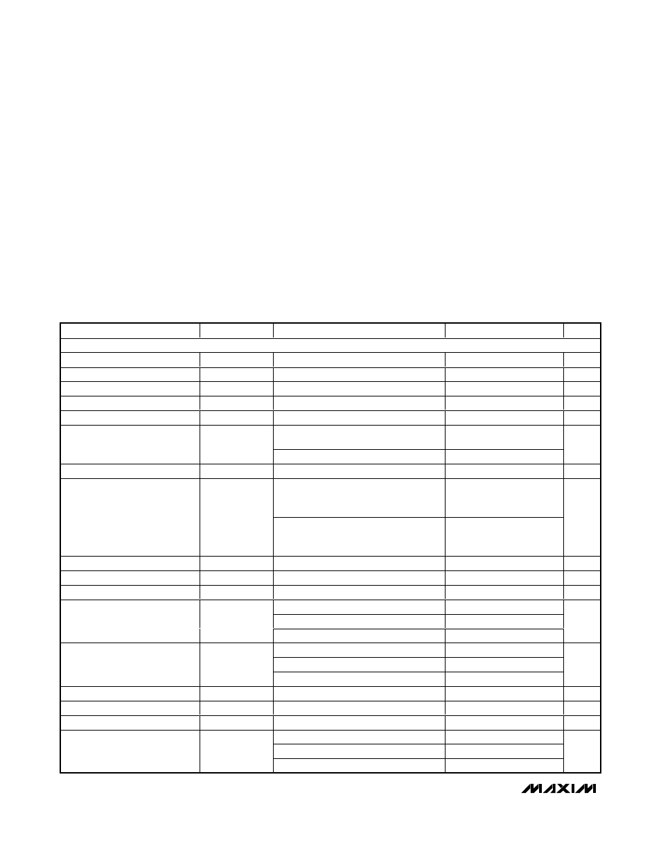
ELECTRICAL CHARACTERISTICS
(V
DD
= 3.3V, SHDN = V
DD
, C
CT
= 470nF, C
CG
= 2µF, GAIN = V
DD
, T
A
= T
MIN
to T
MAX
, unless otherwise specified. Typical values are
at T
A
= +25°C.) (Note 1)
Stresses beyond those listed under “Absolute Maximum Ratings” may cause permanent damage to the device. These are stress ratings only, and functional
operation of the device at these or any other conditions beyond those indicated in the operational sections of the specifications is not implied. Exposure to
absolute maximum rating conditions for extended periods may affect device reliability.
V
DD
to GND ..............................................................-0.3V to +6V
All Other Pins to GND.................................-0.3V to (V
DD
+ 0.3V)
Output Short-Circuit Duration.....................................Continuous
Continuous Current (OUT, MICBIAS) .............................±100mA
All Other Pins ....................................................................±20mA
Continuous Power Dissipation (T
A
= +70°C)
12-Bump UCSP (derate 6.5mW/°C above +70°C).......518mW
14-Pin TDFN (derate 16.7mW/°C above +70°C) ....1481.5mW
Operating Temperature Range ...........................-40°C to +85°C
Junction Temperature ......................................................+150°C
Lead Temperature (soldering, 10s) .................................+300°C
Bump Temperature (soldering) Reflow............................+235°C
PARAMETER
SYMBOL
CONDITIONS
MIN
TYP
MAX
UNITS
GENERAL
Operating Voltage
V
DD
Guaranteed by PSRR test
2.7
5.5
V
Supply Current
I
DD
3.1
6
mA
Shutdown Supply Current
I
SHDN
0.01
1
µA
Input-Referred Noise Density
e
n
BW = 20kHz, all gain settings
30
nV/
√Hz
Output Noise
BW = 20kHz
430
µV
RMS
BW = 22Hz to 22kHz
(500mV
RMS
output signal)
61
Signal-to-Noise Ratio
SNR
A-weighted
64
dB
Dynamic Range
DR
(Note 2)
60
dB
f
IN
= 1kHz, BW = 20Hz to 20kHz,
R
L
= 10k
Ω, V
TH
= 1V (threshold = 2V
P-
P
), V
IN
= 0.5mV
RMS
, V
CT
= 0V
0.04
Total Harmonic Distortion Plus
Noise
THD+N
f
IN
= 1kHz, BW = 20Hz to 20kHz,
R
L
= 10k
Ω, V
TH
= 0.1V (threshold =
200mV
P-P
), V
IN
= 30mV
RMS
, V
CT
= 2V
0.2
%
Amplifier Input BIAS
V
IN
1.14
1.23
1.32
V
Maximum Input Voltage
V
IN_MAX
1% THD
100
mV
P-P
Input Impedance
Z
IN
100
k
Ω
GAIN = V
DD
39.5
40
40.5
GAIN = GND
49.5
50
50.6
Maximum Gain
A
GAIN = unconnected
59.5
60
60.5
dB
GAIN = V
DD
18.7
20
20.5
GAIN = GND
29.0
30
30.8
Minimum Gain
GAIN = unconnected
38.7
40
40.5
dB
Maximum Output Level
V
OUT_RMS
1% THD+N, V
TH
= MICBIAS
0.707
V
RMS
Regulated Output Level
AGC enabled, V
TH
= 0.7V
1.26
1.40
1.54
V
P-P
AGC Attack Time
t
ATTACK
C
T
= 470nF (Note 3)
1.1
ms
A/R = GND
1:500
A/R = V
DD
1:2000
Attack/Release Ratio
A/R
A/R = unconnected
1:4000
ms/ms