3 wiring diagram – Rainbow Electronics AT42QT4120 User Manual
Page 3
3
9506AS–AT42–10/08
AT42QT4120
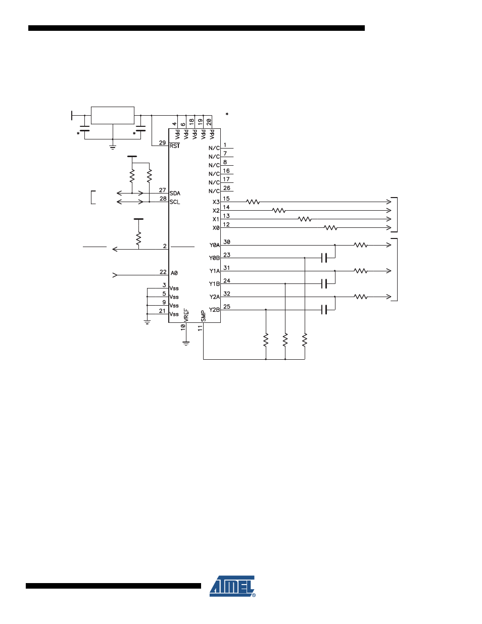
1.3
Wiring Diagram
Figure 1-1.
Wiring Diagram
Suggested regulator manufacturers:
• Torex (XC6215 series)
• Seiko (S817 series)
• BCDSemi (AP2121 series)
Rp
Rp
Rs2
Rs0
Ry2
Ry1
Ry0
SCL
SDA
VREG
Rx2
Rc
VDD
Rs1
Rx3
Cs2
Cs1
Cs0
Rx0
Vunreg
VDD
Rx1
N/C
N/C
CHANGE
QT4120
N/C
N/C
N/C
N/C
VDD
M
A
T
R
IXYS
C
A
N
IN
follow regulator manufacturer's recommended values for input
and output bypass capacitors; keep output capacitor close to
pins 4 and 6. If not possible, add a 100nF capacitor next to those pins.
MA
TRIX
X
DRIVE
NOTES:
1) The central pad on the underside of the chip
is a Vss pin and should be connected to ground.
Do not put any other tracks underneath
the body of the chip.
2) It is important to place all Cs, Rs, Rx and Ry
components physically near to the chip.
I C-COMPATIBLE
2
I C-COMPATIBLE
2
ADDRESS SELECT
CHANGE