Test circuits/timing diagrams, Electrical characteristics (continued) – Rainbow Electronics MAX14998 User Manual
Page 3
Two-Lane and Four-Lane DisplayPort Passive
Switches with Separate AUX/HPD Control
MAX4998/MAX14998
_______________________________________________________________________________________ 3
ELECTRICAL CHARACTERISTICS (continued)
(V
DD
= +3.3V Q10%, T
A
= T
MIN
to T
MAX,
unless otherwise noted. Typical values are at V
DD
= +3.3V, T
A
= +25NC, unless otherwise
noted.) (Note 3)
Note 3: All units are 100% production tested at T
A
= +85NC. Limits over the operating temperature range are guaranteed by
design and characterization and are not production tested.
Note 4: DR
ON
= R
ON(MAX)
- R
ON(MIN)
.
Note 5: Guaranteed by design. Not production tested.
Note 6: Flatness is defined as the difference between the maximum and minimum value of on-resistance as measured over the
specified analog signal range.
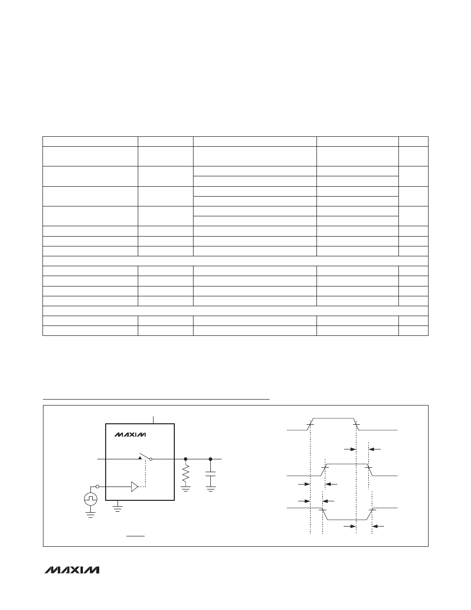
Test Circuits/Timing Diagrams
Figure 1. Switching Time
t
r
< 5ns
t
f
< 5ns
50%
V
IL
LOGIC
INPUT
SEL
R
L
COM_
GND
SEL_
C
L
INCLUDES FIXTURE AND STRAY CAPACITANCE.
V
N_
V
IH
0V
0V
NO_ OR NC_
0.9 x V
OUT
0.9 x V
OUT
0.9 x V
OUT
0.9 x V
OUT
t
ON_SEL
t
OFF_SEL
V
OUT
SWITCH
OUTPUT
COM_
SWITCH
OUTPUT
COM_
LOGIC
INPUT
SEL_
V
DD
C
L
+3.3V
V
OUT
t
ON_SEL
t
OFF_SEL
MAX4998/MAX14998
V
OUT
= V
N_
R
L
R
L
+ R
ON
(
)
PARAMETER
SYMBOL
CONDITIONS
MIN
TYP
MAX
UNITS
SEL1 and SEL2 to Switch
Turn-Off Time
t
OFF_SEL
V
NO_
or V
NC_
= +1.0V, R
L
= 50I,
C
L
= 100pF (Figure 1)
5
50
ns
Differential Insertion Loss
S
DD21
f = 0.8GHz (Figure 2)
-0.67
dB
f = 1.35GHz (Figure 2)
-0.95
Differential Crosstalk
S
DDCTK
f = 0.8GHz (Figure 2)
-37
dB
f = 1.35GHz (Figure 2)
-34
Differential Return Loss
S
DD11
f = 0.8GHz (Figure 2)
-20
dB
f = 1.35GHz (Figure 2)
-14
Signal Data Rate
BR
R
S
= R
L
= 100I balanced
17
Gbps
Differential -3dB Bandwidth
f
-3BW
R
S
= R
L
= 100I balanced
8.5
GHz
Differential Off-Isolation
S
DD21_OFF
f = 1.35GHz (Figure 2)
-28
dB
LOGIC INPUT (SEL1, SEL2)
Input Logic-High
V
IH
1.4
V
Input Logic-Low
V
IL
0.5
V
Input Logic Hysteresis
V
HYST
100
mV
Input Leakage Current
I
IN
V
SEL_
= 0V or V
DD
-1
+1
F
A
POWER SUPPLY
Power-Supply Range
V
DD
3.0
3.6
V
V
DD
Supply Current
I
DD
V
SEL_
= 0V or V
DD
500
850
F
A