Absolute maximum ratings, Electrical characteristics – Rainbow Electronics MAX9944 User Manual
Page 2
MAX9943/MAX9944
High-Voltage, Precision, Low-Power Op Amps
2
_______________________________________________________________________________________
ABSOLUTE MAXIMUM RATINGS
Stresses beyond those listed under “Absolute Maximum Ratings” may cause permanent damage to the device. These are stress ratings only, and functional
operation of the device at these or any other conditions beyond those indicated in the operational sections of the specifications is not implied. Exposure to
absolute maximum rating conditions for extended periods may affect device reliability.
Supply Voltage (V
CC
to V
EE
) ..................................-0.3V to +40V
All Other Pins (Note 1) .....................(V
EE
- 0.3V) to (V
CC
+ 0.3V)
OUT Short-Circuit Current Duration
8-Pin µMAX (V
CC
- V
EE
≤ 20V)...............................................3s
8-Pin µMAX (V
CC
- V
EE
> 20V) ................................Momentary
6-Pin TDFN (V
CC
- V
EE
≤ 20V) .............................................60s
6-Pin TDFN (V
CC
- V
EE
> 20V)...............................................2s
8-Pin SO (V
CC
- V
EE
≤ 20V) .................................................60s
8-Pin SO (V
CC
- V
EE
> 20V)...................................................2s
8-Pin TDFN (V
CC
- V
EE
≤ 20V) .............................................60s
8-Pin TDFN (V
CC
- V
EE
> 20V)...............................................2s
Continuous Input Current (Any Pins) ................................±20mA
Thermal Limits (Note 2)
Multiple Layer PCB
Continuous Power Dissipation (T
A
= +70°C)
8-Pin µMAX (derate 4.8mW/°C above +70°C) ...........387.8mW
θ
JA
.........................................................................206.3°C/W
θ
JC
..............................................................................42°C/W
6-Pin TDFN-EP (derate 23.8mW/°C above +70°C) ..1904.8mW
θ
JA
..............................................................................42°C/W
θ
JC
................................................................................9°C/W
8-Pin SO (derate 7.6mW/°C above +70°C)...................606.1W
θ
JA
............................................................................132°C/W
θ
JC
..............................................................................38°C/W
8-Pin TDFN-EP (derate 24.4mW/°C above +70°C) ..1951.2mW
θ
JA
..............................................................................41°C/W
θ
JC
................................................................................8°C/W
Operating Temperature Range .........................-40°C to +125°C
Junction Temperature ......................................................+150°C
Lead Temperature (soldering, 10s) .................................+300°C
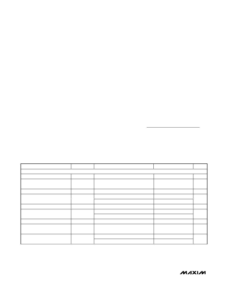
PARAMETER
SYMBOL
CONDITIONS
MIN
TYP
MAX
UNITS
DC CHARACTERISTICS
Operating Supply Voltage Range
V
SUPPLY
Guaranteed by PSRR test
±3
±19
V
Quiescent Supply Current per
Amplifier
I
CC
550
950
µA
Power-Supply Rejection Ratio
PSRR
V
S
= ±3V to ±19V
105
130
dB
T
A
= +25°C
20
100
Input Offset Voltage
V
OS
T
A
= -40°C to +125°C
240
µV
Input Offset Voltage Drift
TCV
OS
0.4
µV/°C
V
EE
+ 0.3V ≤ V
CM
≤ V
CC
- 1.8V
4
20
Input Bias Current
I
BIAS
V
EE
≤ V
CM
≤ V
CC
- 1.8V
90
nA
Input Offset Current
I
OS
V
EE
≤ V
CM
≤ V
CC
- 1.8V
1
10
nA
Input Voltage Range
V
IN+
, V
IN-
Guaranteed by CMRR test,
T
A
= -40°C to +125°C
V
EE
V
CC
-
1.8
V
V
EE
+ 0.3V ≤ V
CM
≤ V
CC
- 1.8V
105
125
Common-Mode Rejection Ratio
CMRR
V
EE
≤ V
CM
≤ V
CC
- 1.8V
105
dB
ELECTRICAL CHARACTERISTICS
(V
CC
= 15V, V
EE
= -15V, V
CM
= 0, R
L
= 10kΩ to GND, GND = 0, T
A
= -40°C to +125°C. Typical values are at T
A
= +25°C, unless oth-
erwise noted.) (Note 3)
Note 1: Operation is limited by thermal limits.
Note 2: Package thermal resistances were obtained using the method described in JEDEC specification JESD51-7, using a four-
layer board. For detailed information on package thermal considerations, refer to
www.maxim-ic.com/thermal-tutorial
.