Rainbow Electronics MAX15026 User Manual
Page 2
MAX15026
Low-Cost, Small, 4.5V to 28V Wide Operating
Range, DC-DC Synchronous Buck Controller
2
_______________________________________________________________________________________
ABSOLUTE MAXIMUM RATINGS
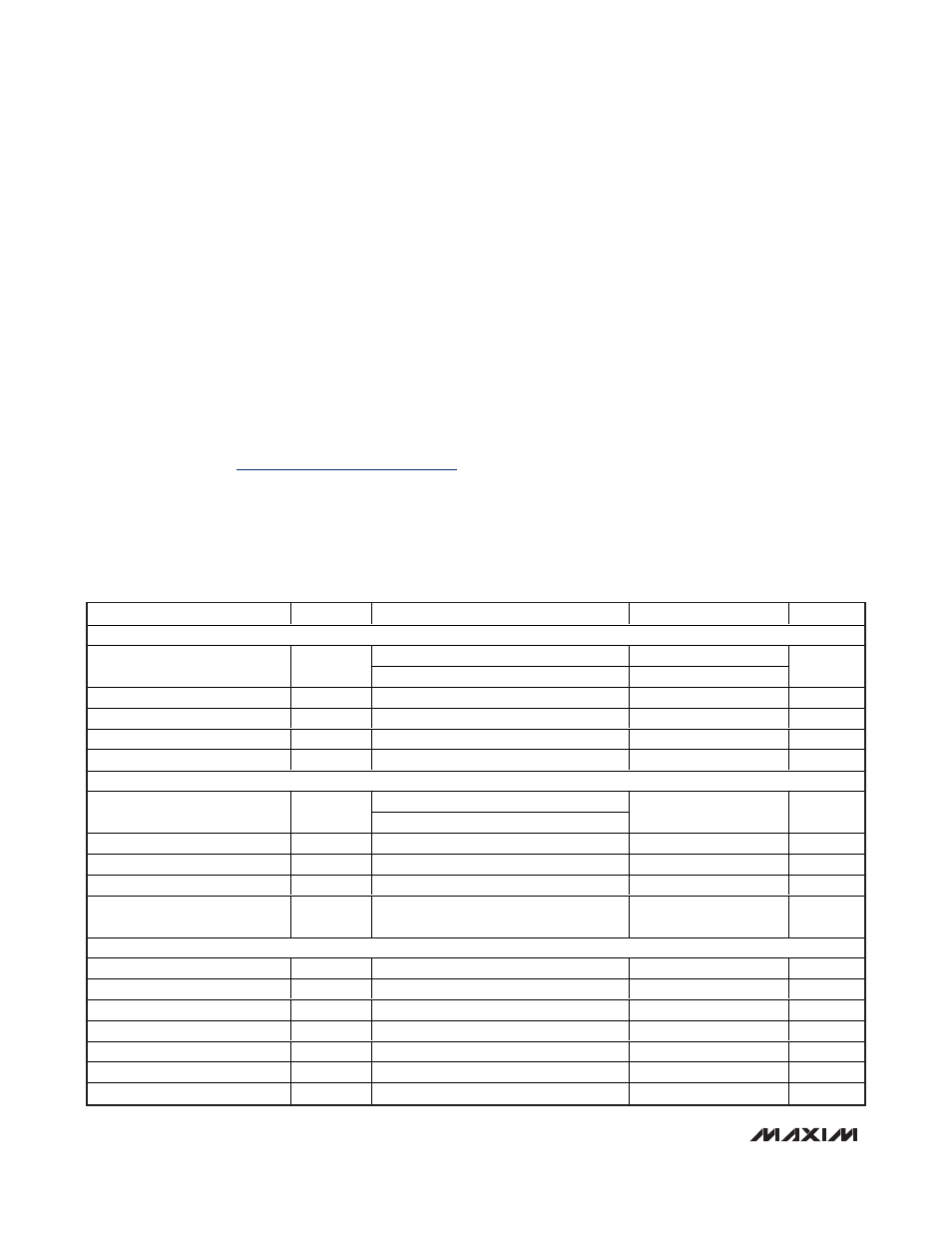
ELECTRICAL CHARACTERISTICS
(V
IN
= 12V, R
RT
= 27k
Ω, R
LIM
= 30k
Ω, C
VCC
= 4.7µF, C
IN
= 1µF, T
A
= -40°C to +85°C, unless otherwise noted. Typical values are at
T
A
= +25°C.) (Note 2)
Stresses beyond those listed under “Absolute Maximum Ratings” may cause permanent damage to the device. These are stress ratings only, and functional
operation of the device at these or any other conditions beyond those indicated in the operational sections of the specifications is not implied. Exposure to
absolute maximum rating conditions for extended periods may affect device reliability.
Note 1: Dissipation wattage values are based on still air with no heatsink. Actual maximum power dissipation is a function of heat
extraction technique and may be substantially higher. Package thermal resistances were obtained using the method
described in JEDEC specification JESD51-7, using a four-layer board. For detailed information on package thermal consid-
erations, refer to
www.maxim-ic.com/thermal-tutorial
.
IN to GND ...............................................................-0.3V to +30V
BST to GND ............................................................-0.3V to +36V
LX to GND .................................................................-1V to +30V
EN to GND................................................................-0.3V to +6V
PGOOD to GND .....................................................-0.3V to +30V
BST to LX..................................................................-0.3V to +6V
DH to LX ...............................................….-0.3V to (V
BST
+ 0.3V)
DRV to GND .............................................................-0.3V to +6V
DL to GND ................................................-0.3V to (V
DRV
+ 0.3V)
V
CC
to GND ...............-0.3V to the lower of +6V and (V
IN
+ 0.3V)
All Other Pins to GND.................................-0.3V to (V
CC
+ 0.3V)
V
CC
Short Circuit to GND ...........................................Continuous
DRV Input Current.............................................................600mA
PGOOD Sink Current ............................................................5mA
Continuous Power Dissipation (T
A
= +70°C) (Note 1)
14-Pin TDFN-EP, Multilayer Board
(derate 24.4mW/°C above +70°C) ..............................1951mW
Operating Temperature Range ...........................-40°C to +85°C
Junction Temperature ......................................................+150°C
Storage Temperature Range .............................-60°C to +150°C
Lead Temperature (soldering, 10s) .................................+300°C
PARAMETER
SYMBOL
CONDITIONS
MIN
TYP
MAX
UNITS
GENERAL
4.5
28
Input Voltage Range
V
IN
V
IN
= V
CC
= V
DRV
4.5
5.5
V
Quiescent Supply Current
V
FB
= 0.9V, no switching
1.75
2.75
mA
Shutdown Supply Current
I
IN_SBY
EN = GND
290
500
µA
Enable to Output Delay
480
µs
V
CC
High to Output Delay
EN = V
CC
375
µs
V
CC
REGULATOR
6V < V
IN
< 28V, I
LOAD
= 25mA
Output Voltage
V
CC
V
IN
= 12V, 1mA < I
LOAD
< 70mA
5.0
5.25
5.5
V
V
CC
Regulator Dropout
V
IN
= 4.5V, I
LOAD
= 70mA
0.28
V
V
CC
Short-Circuit Output Current
V
IN
= 5V
100
200
300
mA
V
CC
Undervoltage Lockout
V
CC_UVLO
V
CC
rising
3.8
4.0
4.2
V
V
CC
Undervoltage Lockout
Hysteresis
400
mV
ERROR AMPLIFIER (FB, COMP)
FB Input Voltage Set-Point
V
FB
582
592
597
mV
FB Input Bias Current
I
FB
V
FB
= 0.6V
-250
+250
nA
FB to COMP Transconductance
g
M
I
COMP
= ±20µA
600
1200
1800
µS
Amplifier Open-Loop Gain
80
dB
Amplifier Unity-Gain Bandwidth
Capacitor from COMP to GND = 50pF
4
MHz
V
COMP-RAMP
Minimum Voltage
160
mV
COMP Source/Sink Current
I
COMP
V
COMP
= 1.4V
50
80
110
µA