Rainbow Electronics MAX15026 User Manual
Page 16
MAX15026
Solving for C
F
:
3) Place a high-frequency pole at f
P1
= 0.5 x f
SW
(to
attenuate the ripple at the switching frequency, f
SW
)
and calculate C
CF
using the following equation:
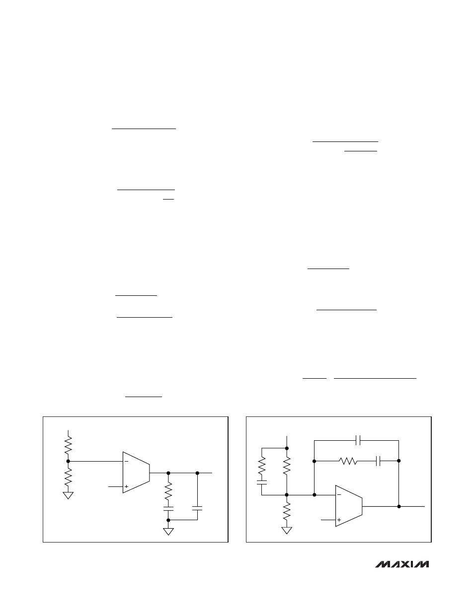
Type III Compensation Network
(See Figure 4)
When using a low-ESR tantalum or ceramic type, the
ESR-induced zero frequency is usually above the tar-
geted zero crossover frequency (f
O
). Use Type III com-
pensation. Type III compensation provides three poles
and two zeros at the following frequencies:
Two midband zeros (f
Z1
and f
Z2
) cancel the pair of
complex poles introduced by the LC filter:
f
P1
= 0
f
P1
introduces a pole at zero frequency (integrator) for
nulling DC output voltage errors:
Depending on the location of the ESR zero (f
ZO
), use
f
P2
to cancel f
ZO
, or to provide additional attenuation of
the high-frequency output ripple:
f
P3
attenuates the high-frequency output ripple.
Place the zeros and poles so the phase margin peaks
around f
O
.
Ensure that R
F
>>2/g
M
and the parallel resistance of R
1
,
R
2
, and R
I
is greater than 1/g
M
. Otherwise, a 180°
phase shift is introduced to the response making the
loop unstable.
Use the following compensation procedure:
1) With R
F
≥ 10kΩ, place the first zero (f
Z1
) at 0.8 x f
PO
.
So:
2) The gain of the modulator (GAIN
MOD
), comprises
the pulse-width modulator, LC filter, feedback
divider, and associated circuitry at the crossover
frequency is:
GAIN
V
V
f
L
C
MOD
IN
RAMP
O
OUT
OUT
=
Ч
Ч
Ч
Ч
1
2
2
(
)
π
C
R
f
F
F
PO
=
Ч
Ч
Ч
1
2
0 8
π
.
f
R
C
f
Z
F
F
PO
1
1
2
0 8
=
Ч
Ч
=
Ч
π
.
f
R
C
C
C
C
P
F
F
CF
F
CF
3
1
2
=
Ч
Ч
Ч
+
π
f
R
C
P
I
I
2
1
2
=
Ч Ч
π
f
R
C
f
C
R
R
Z
F
F
Z
I
I
1
2
1
1
2
1
2
=
Ч
Ч
=
Ч
Ч
+
π
π
(
)
C
R
f
C
CF
F
SW
F
=
Ч
Ч
−
1
1
π
C
R
f
F
F
PO
=
Ч
Ч
Ч
1
2
0 75
π
.
Low-Cost, Small, 4.5V to 28V Wide Operating
Range, DC-DC Synchronous Buck Controller
16
______________________________________________________________________________________
V
REF
R
1
V
OUT
R
2
g
M
R
F
COMP
C
F
C
CF
Figure 3. Type II Compensation Network
V
REF
g
M
R
1
R
2
V
OUT
R
I
COMP
C
I
C
CF
R
F
C
F
Figure 4. Type III Compensation Network