Pinout and schematic, 1 pinout configuration, 2 pin descriptions – Rainbow Electronics AT42QT5320 User Manual
Page 2: Qt5320
2
9509AS–AT42–10/08
QT5320
1.
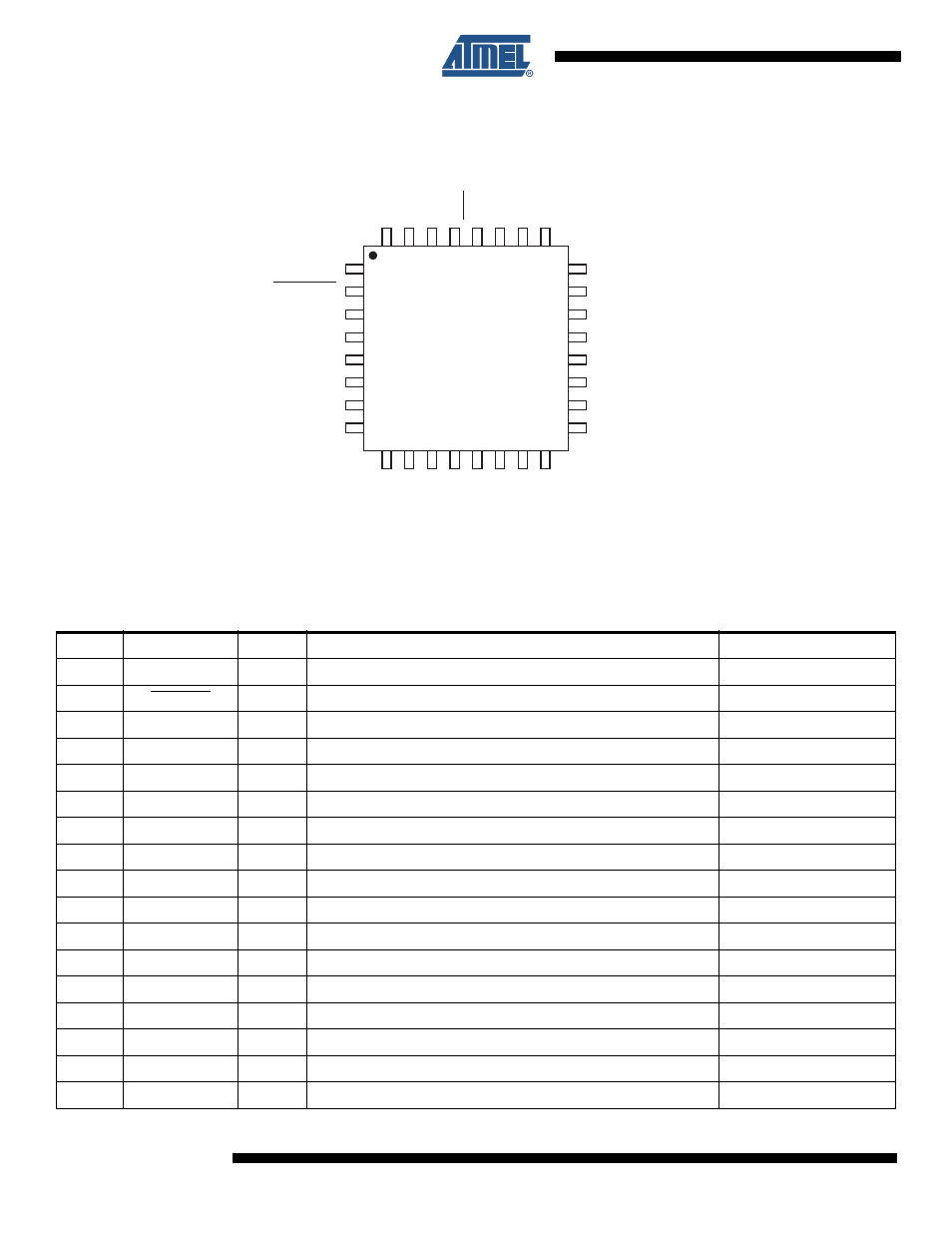
Pinout and Schematic
1.1
Pinout Configuration
1.2
Pin Descriptions
Table 1-1.
Pin Listing
Pin
Name
Type
Comments
If Unused, Connect To...
1
Y3A
I
Y line connection
Leave open
2
CHANGE
OD
State change notification
–
3
Vss
P
Supply ground
–
4
Vdd
P
Power
–
5
Vss
P
Supply ground
–
6
Vdd
P
Power
–
7
X6
O
X matrix drive line
Leave open
8
X7
O
X matrix drive line
Leave open
9
TRIGGER
I
Trigger input (active low)
Vdd or Vss
10
Vref
I
Supply ground
–
11
SMP
O
Sample output.
–
12
X0
O
X matrix drive line
Leave open
13
X1
O
X matrix drive line
Leave open
14
X2
O
X matrix drive line
Leave open
15
X3
O
X matrix drive line
Leave open
16
X4
O
X matrix drive line
Leave open
17
X5
O
X matrix drive line
Leave open
Y2A
Y1A
Y0A
RST
SCL
SDA
Y3B
Y2B
TRIGGER
VREF
SMP
X0
X1
X2
X3
X4
Y3A
CHANGE
Vss
Vdd
Vss
Vdd
X6
X7
X5
Vdd
Vdd
Vss
A0
Y0B
Y1B
1
2
3
4
5
6
7
8
17
18
19
20
21
22
23
24
32 31 30 29 28 27 26 25
9 10 11
16
15
14
13
12
QT5320
FORCE_S