Connection diagrams, Pin descriptions – Rainbow Electronics ADC10664 User Manual
Page 9
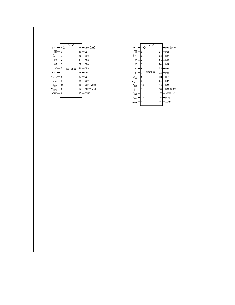
Connection Diagrams
Dual-In-Line Package
TL H 11192 – 10
Top View
Dual-In-Line Package
TL H 11192 – 11
Top View
Pin Descriptions
DV
CC
AV
CC
These are the digital and analog positive sup-
ply voltage inputs They should always be
connected to the same voltage source but
are brought out separately to allow for sepa-
rate bypass capacitors
Each supply pin
should be bypassed with a 0 1 mF ceramic
capacitor in parallel with a 10 mF tantalum
capacitor to ground
INT
This is the active low interrupt output INT
goes low at the end of each conversion and
returns to a high state following the rising
edge of RD
S H
This is the Sample Hold control input When
this pin is forced low (and CS is low) it caus-
es the analog input signal to be sampled and
initiates a new conversion
RD
This is the active low Read control input
When this RD and CS are low any data pres-
ent in the output registers will be placed on
the data bus
CS
This is the active low Chip Select control in-
put When low this pin enables the RD and
S H pins
S0 S1
These pins select the analog input that will be
connected to the A D during the conversion
The input is selected based on the state of
S0 and S1 when S H makes its High-to-Low
transition (See the Timing Diagrams) The
ADC10664 includes both S0 and S1 The
ADC10662 includes just S0
V
REF
b
These are the reference voltage inputs They
V
REF
a
may be placed at any voltage between GND
and V
CC
but V
REF
a
must be greater than
V
REF
b
An input voltage equal to V
REF
b
produces an output code of 0 and an input
voltage equal to (V
REF
a
b
1 LSB) produces
an output code of 1023
V
IN0
V
IN1
These are the analog input pins
The
V
IN2
V
IN3
ADC10662 has two inputs (V
IN0
and V
IN1
)
and the ADC10664 has four inputs (V
IN0
V
IN1
V
IN2
and V
IN3
) The impedance of the
source should be less than 500X for best ac-
curacy and conversion speed For accurate
conversions no input pin (even one that is
not selected) should be driven more than
50 mV above V
CC
or 50 mV below ground
GND AGND These are the power supply ground pins The
DGND
ADC10662 and ADC10664 have separate
analog and digital ground pins (AGND and
DGND) for separate bypassing of the analog
and digital supplies The ground pins should
be connected to a stable noise-free system
ground Both pins should be returned to the
same potential
DB0 – DB9
These are the TRI-STATE output pins
SPEED ADJ
By connecting a resistor between this pin and
ground the conversion time can be reduced
The specifications listed in the table of Elec-
trical Characteristics apply for a speed adjust
resistor (R
SA
) equal to 14 0 kX (Mode 1) or
8 26 kX (Mode 2) See the Typical Perform-
ance Curves and the table of Electrical Char-
acteristics
9