Applications information – Rainbow Electronics ADC10664 User Manual
Page 11
Applications Information
1 0 MODES OF OPERATION
The ADC10662 and ADC10664 have two basic digital inter-
face modes
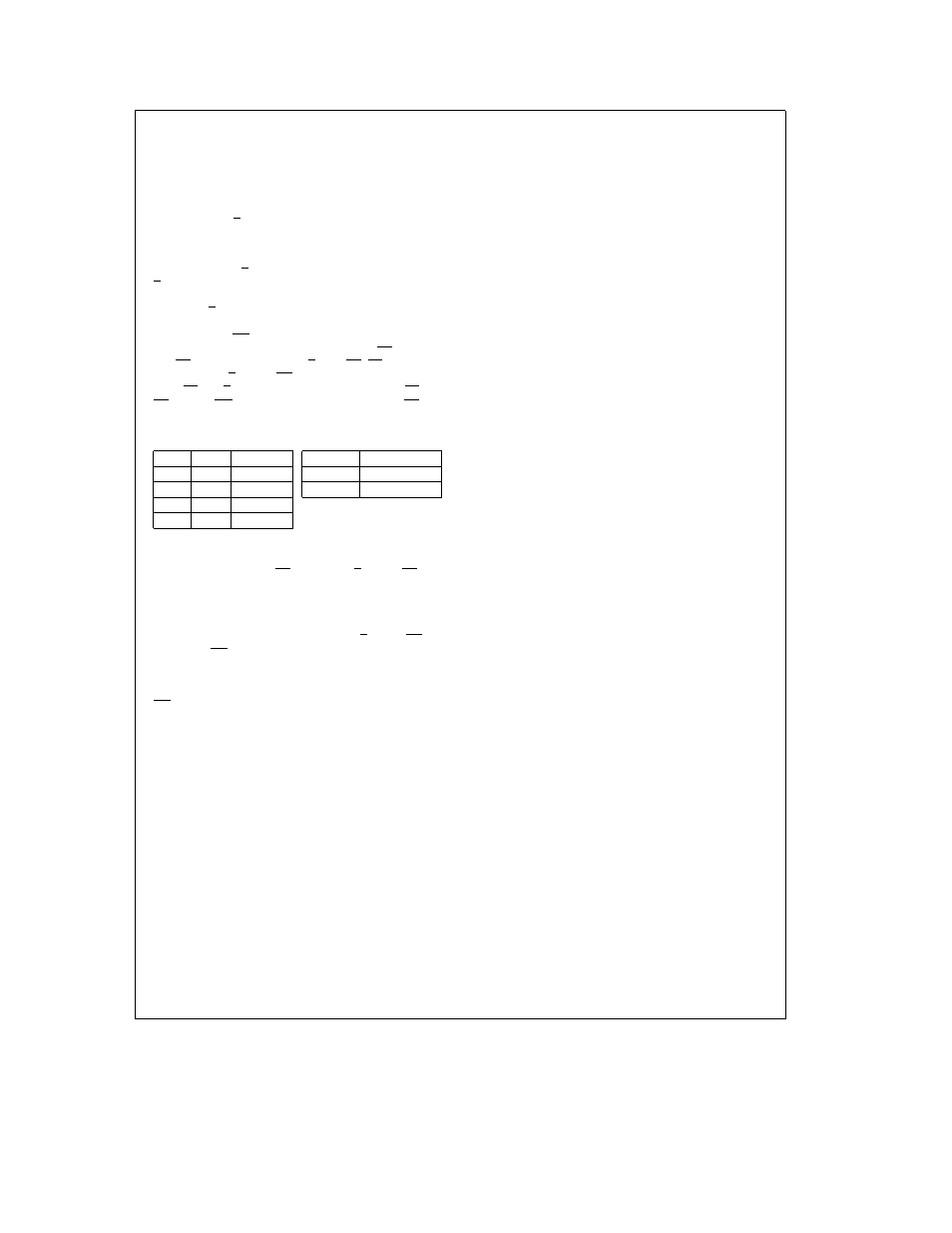
Figure 1
and
Figure 2
are timing diagrams for
the two modes The ADC10662 and ADC10664 have input
multiplexers that are controlled by the logic levels on pins
S
0
and S
1
when S H goes low Table I is a truth table show-
ing how the input channnels are assigned
Mode 1
In this mode the S H pin controls the start of conversion
S H is pulled low for a minimum of 150 ns This causes the
comparators in the ‘‘coarse’’ flash converter to become ac-
tive When S H goes high the result of the coarse conver-
sion is latched and the ‘‘fine’’ conversion begins After
360 ns (typical) INT goes low indicating that the conversion
results are latched and can be read by pulling RD low Note
that CS must be low to enable S H or RD CS is internally
‘‘ANDed’’ with S H and RD the input voltage is sampled
when CS and S H are low and data is read when CS and
RD are low INT is reset high on the rising edge of RD
TABLE I Input Multiplexer Programming
ADC10664
ADC10662
S
1
S
0
Channel
S
0
Channel
0
0
V
IN0
0
V
IN0
0
1
V
IN1
1
V
IN1
1
0
V
IN2
(b)
1
1
V
IN3
(a)
Mode 2
In Mode 2 also called ‘‘RD mode’’ the S H and RD pins
are tied together A conversion is initiated by pulling both
pins low The A D converter samples the input voltage and
causes the coarse comparators to become active An inter-
nal timer then terminates the coarse conversion and begins
the fine conversion 470 ns (typical) after S H and RD are
pulled low INT goes low indicating that the conversion is
completed Approximately 20 ns later the data appearing on
the TRI-STATE output pins will be valid Note that data will
appear on these pins throughout the conversion but until
INT goes low the data at the output pins will be the result of
the previous conversion
2 0 REFERENCE CONSIDERATIONS
The ADC10662 and ADC10664 each have two reference
inputs These inputs V
REF
a
and V
REF
b
are fully differen-
tial and define the zero to full-scale range of the input signal
The reference inputs can be connected to span the entire
supply voltage range (V
REF
b
e
0V V
REF
a
e
V
CC
) for
ratiometric applications or they can be connected to differ-
ent voltages (as long as they are between ground and V
CC
)
when other input spans are required Reducing the overall
V
REF
span to less than 5V increases the sensitivity of the
converter (e g
if V
REF
e
2V then 1 LSB e 1 953 mV)
Note however that linearity and offset errors become larg-
er when lower reference voltages are used See the Typical
Performance Curves for more information For this reason
reference voltages less than 2V are not recommended
In most applications V
REF
b
will simply be connected to
ground but it is often useful to have an input span that is
offset from ground This situation is easily accommodated
by the reference configuration used in the ADC10662 and
ADC10664 V
REF
b
can be connected to a voltage other
than ground as long as the voltage source connected to this
pin is capable of sinking the converter’s reference current
(12 5 mA Max
V
REF
e
5V) If V
REF
b
is connected to a
voltage other than ground bypass it with multiple capaci-
tors
Since the resistance between the two reference inputs can
be as low as 400X the voltage source driving the reference
inputs should have low output impedance Any noise on ei-
ther reference input is a potential cause of conversion er-
rors so each of these pins must be supplied with a clean
low noise voltage source Each reference pin should be by-
passed with a 10 mF tantalum and a 0 1 mF ceramic
3 0 THE ANALOG INPUT
The ADC10662 and ADC10664 sample the analog input
voltage once every conversion cycle When this happens
the input is briefly connected to an impedance approximate-
ly equal to 600X in series with 35 pF Short-duration current
spikes can therefore be observed at the analog input during
normal operation These spikes are normal and do not de-
grade the converter’s performance
Large source impedances can slow the charging of the
sampling capacitors and degrade conversion accuracy
Therefore only signal sources with output impedances less
than 500X should be used if rated accuracy is to be
achieved at the minimum sample time (250 ns maximum) If
the sampling time is increased the source impedance can
be larger If a signal source has a high output impedance its
output should be buffered with an operational amplifier The
operational amplifier’s output should be well-behaved when
driving a switched 35 pF 600X load Any ringing or voltage
shifts at the op amp’s output during the sampling period can
result in conversion errors
Correct conversion results will be obtained for input volt-
ages greater than GND b 50 mV and less than V
a
a
50 mV Do not allow the signal source to drive the analog
input pin more than 300 mV higher than AV
CC
and DV
CC
or
more than 300 mV lower than GND If an analog input pin is
forced beyond these voltages the current flowing through
the pin should be limited to 5 mA or less to avoid permanent
damage to the IC The sum of all the overdrive currents into
all pins must be less than 20 mA When the input signal is
expected to extend more than 300 mV beyond the power
supply limits some sourt of protection scheme should be
used A simple network using diodes and resistors is shown
in
Figure 4
11