Dc electrical characteristics, Ac electrical characteristics – Rainbow Electronics ADC10664 User Manual
Page 3
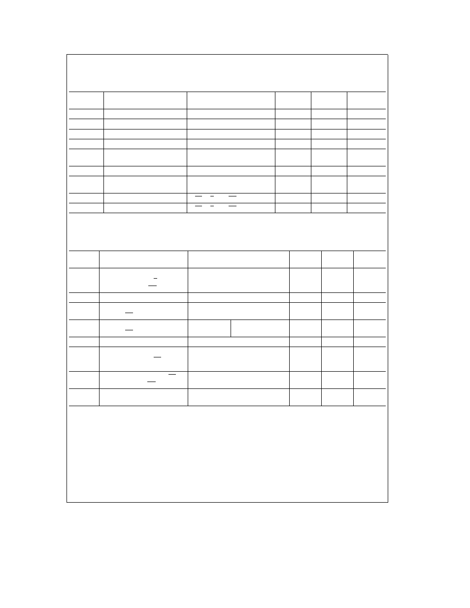
DC Electrical Characteristics
The following specifications apply for V
a
e a
5V V
REF(
a
)
e
5V V
REF(
b
)
e
GND and Speed Adjust pin connected to ground
through a 14 0 kX resistor (Mode 1) or an 8 26 kX resistor (Mode 2) unless otherwise specified Boldface limits apply for T
A
e
T
J
e
T
MIN
to T
MAX
all other limits T
A
e
T
J
e a
25 C
Symbol
Parameter
Conditions
Typical
Limit
Units
(Note 7)
(Note 8)
(Limits)
V
IN(1)
Logical ‘‘1’’ Input Voltage
V
a
e
5 5V
2 0
V (min)
V
IN(0)
Logical ‘‘0’’ Input Voltage
V
a
e
4 5V
0 8
V (max)
I
IN(1)
Logical ‘‘1’’ Input Current
V
IN(1)
e
5V
0 005
3 0
m
A (max)
I
IN(0)
Logical ‘‘0’’ Input Current
V
IN(0)
0V
b
0 005
b
3 0
m
A (max)
V
OUT(1)
Logical ‘‘1’’ Output Voltage
V
a
e
4 5V I
OUT
e b
360 mA
2 4
V (min)
V
a
e
4 5V I
OUT
e b
10 mA
4 25
V (min)
V
OUT(0)
Logical ‘‘0’’ Output Voltage
V
a
e
4 5V I
OUT
e
1 6 mA
0 4
V (max)
I
OUT
TRI-STATE Output Current
V
OUT
e
5V
0 1
50
m
A (max)
V
OUT
e
0V
b
0 1
b
50
m
A (max)
DI
CC
DV
CC
Supply Current
CS e S H e RD e 0
1 0
2
mA (max)
AI
CC
AV
CC
Supply Current
CS e S H e RD e 0
30
45
mA (max)
AC Electrical Characteristics
The following specifications apply for V
a
e
a
5V t
r
e
t
f
e
20 ns V
REF(
a
)
e
5V V
REF(
b
)
e
GND and Speed Adjust pin
connected to ground through a 14 0 kX resistor (Mode 1) or an 8 26 kX resistor (Mode 2) unless otherwise specified Boldface
limits apply for T
A
e
T
J
e
T
MIN
to T
MAX
all other limits T
A
e
T
J
e a
25 C
Symbol
Parameter
Conditions
Typical
Limit
Units
(Note 7)
(Note 8)
(Limits)
t
CONV
Mode 1 Conversion Time
CIN CIWM Suffixes
from Rising Edge of S H
360
466
ns (max)
to Falling Edge of INT
t
CRD
Mode 2 Conversion Time
CIN CIWM Suffixes
470
610
ns (max)
t
ACC1
Access Time (Delay from Falling
Mode 1 C
L
e
100 pF
30
50
ns (max)
Edge of RD to Output Valid)
t
ACC2
Access Time (Delay from Falling
Mode 2
CIN CIWM Suffixes
475
616
ns (max)
Edge of RD to Output Valid)
C
L
e
100 pF
t
SH
Minimum Sample Time
Mode 1
(Figure 1)
(Note 9)
150
ns (max)
t
1H
t
0H
TRI-STATE Control (Delay
R
L
e
1k C
L
e
10 pF
from Rising Edge of RD
30
60
ns (max)
to High-Z State)
t
INTH
Delay from Rising Edge of RD
C
L
e
100 pF
25
50
ns (max)
to Rising Edge of INT
t
P
Delay from End of Conversion
50
ns (max)
to Next Conversion
3