Rainbow Electronics MAX9920 User Manual
Page 2
MAX9918/MAX9919/MAX9920
-20V to +75V Input Range, Precision
Uni-/Bidirectional, Current-Sense Amplifiers
2
_______________________________________________________________________________________
ABSOLUTE MAXIMUM RATINGS
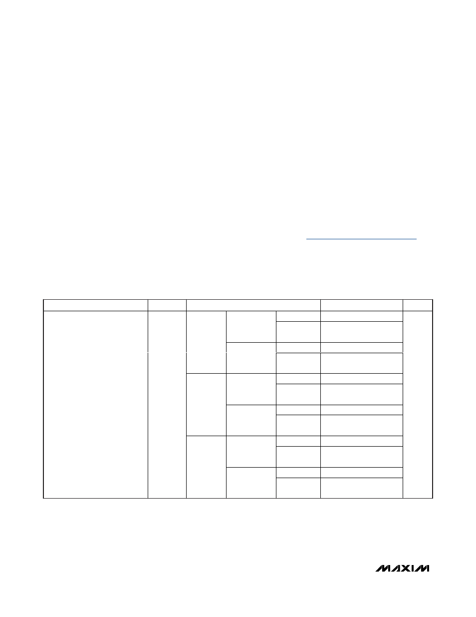
ELECTRICAL CHARACTERISTICS
(V
CC
= 5V, V
RS+
= V
RS-
= +14V, V
SENSE
= (V
RS+
- V
RS-
) = 0V, V
SHDN
= V
GND
= 0V, V
REFIN
= V
CC
/2, R
L
= 100kΩ; for MAX9918, A
V
=
90V/V, R2/R1 = 89kΩ/1kΩ; for MAX9920, A
V
= 20V/V, R2/R1 = 79kΩ/1kΩ; T
A
= -40°C to +125°C, unless otherwise noted. Typical val-
ues are at T
A
= +25°C.) (Note 1)
Stresses beyond those listed under “Absolute Maximum Ratings” may cause permanent damage to the device. These are stress ratings only, and functional
operation of the device at these or any other conditions beyond those indicated in the operational sections of the specifications is not implied. Exposure to
absolute maximum rating conditions for extended periods may affect device reliability.
V
CC
to GND ..............................................................-0.3V to +6V
RS+, RS- to GND (V
CC
= 5V) ..................................-30V to +80V
RS+, RS- to GND (V
CC
= 0V) .............-15V to +80V (15 minutes)
Differential Input Voltage (V
RS+
- V
RS-
)
(MAX9918/MAX9919).................................±15V (Continuous)
Differential Input Voltage
(V
RS+
- V
RS-
) (MAX9920) .............................±5V (Continuous)
REFIN, FB, OUT to GND.............................-0.3V to (V
CC
+ 0.3V)
SHDN to GND.........................................................-0.3V to +20V
Output Short Circuit to V
CC
or GND...........................Continuous
Continuous Current into Any Pin
(Not to exceed package power dissipation) ................±20mA
Continuous Power Dissipation (T
A
= +70°C)
8-Pin SOIC-EP (derate 24.4mW/°C above +70°C) .1951.2mW**
SOIC Package Junction-to-Ambient
Thermal Resistance (
θ
JA
) (Note 1)...............................41°C/W
Junction Temperature ......................................................+150°C
Storage Temperature Range .............................-65°C to +150°C
Reflow Soldering Temperature ........................................+260°C
Lead Temperature (soldering, 10s) .................................+300°C
PARAMETER
SYMBOL
CONDITIONS
MIN
TYP
MAX
UNITS
T
A
= +25°C
±0.14
±0.4
V
RS+
= V
RS-
=
+14V, V
REFIN
= 0V
T
A
= -40°C
to +125°C
±0.7
T
A
= +25°C
±0.08
±0.4
MAX9918
V
RS+
= V
RS-
=
-2V, V
REFIN
=
0V
T
A
= -40°C
to +125°C
±1.3
T
A
= +25°C
±0.18
±0.4
V
RS+
= V
RS-
=
+14V, V
REFIN
= 0V
T
A
= -40°C
to +125°C
±0.9
T
A
= +25°C
±0.11
±0.4
MAX9919_
V
RS+
= V
RS-
=
-2V, V
REFIN
=
0V
T
A
= -40°C
to +125°C
±1.0
T
A
= +25°C
±0.48
±1.2
V
RS+
= V
RS-
=
+14V, V
REFIN
= 0V
T
A
= -40°C
to +125°C
±3.0
T
A
= +25°C
±0.10
±0.9
Input Offset Voltage (Note 2)
V
OS
MAX9920
V
RS+
= V
RS-
=
-2V, V
REFIN
=
0V
T
A
= -40°C
to +125°C
±3.5
mV
Note 1: Package thermal resistances were obtained using the method described in JEDEC specification JESD51-7, using a four-
layer board. For detailed information on package thermal considerations, refer to
www.maxim-ic.com/thermal-tutorial
.
**
As per JEDEC51 Standard (multilayer board).