Detailed description, Typical operating characteristics (continued), Pin description – Rainbow Electronics MAX4198_MAX4199 User Manual
Page 9: Input stage
_______________Detailed Description
The MAX4198/MAX4199 are precision low-power differ-
ential amplifiers with factory-trimmed internal gain-set-
ting resistors. The MAX4198 is trimmed to a gain of
+1V/V and the MAX4199 is trimmed to a gain of +10V/V.
Input Stage
The
Functional Diagram
shows the internal structure of
the MAX4198/MAX4199. Although the resistors are pre-
cision matched, their absolute value varies by ±25%.
The typical input impedance for the MAX4198 is 50k
Ω
for the noninverting input and 25k
Ω
for the inverting
input. The typical input impedance for the MAX4199 is
275k
Ω
for the noninverting input and 25k
Ω
for the
inverting input.
The common-mode inputs of the internal op amp can
range from V
EE
to (V
CC
- 1.1V). Although the inputs to
the internal op amp are not rail-to-rail, the internal resis-
tors form a voltage divider that extends the input com-
mon-mode range beyond-the-rails for the MAX4198.
The overall input range of the MAX4198 extends 100mV
beyond-the-rails without adversely affecting common-
mode rejection or undergoing phase reversal (V
CC
=
5V). The MAX4199 input common-mode range extends
from 100mV below the negative rail to (V
CC
- 1V) (see
the Input Common-Mode Voltage Range vs. Supply
Voltage graph in the
Typical Operating Characteristics
).
MAX4198/MAX4199
Micropower, Single-Supply, Rail-to-Rail
Precision Differential Amplifiers
_______________________________________________________________________________________
9
-0.5
1.5
0.5
4.5
3.5
2.5
7.5
6.5
5.5
2
4
3
5
6
7
8
MAX4199
INPUT COMMON-MODE RANGE vs.
SUPPLY VOLTAGE
MAX4198toc28
SUPPLY VOLTAGE (V)
INPUT COMMON-MODE VOLTAGE (V)
V
REF
= V
CC
/2
Typical Operating Characteristics (continued)
(V
CC
= +5V, V
EE
= 0V, R
L
= 25k
Ω
to V
CC
/ 2, V
SHDN
= V
CC
- 1.5V, small-signal V
OUT
= 100mVp-p, large-signal V
OUT
= 1Vp-p,
T
A
= +25°C, unless otherwise noted.)
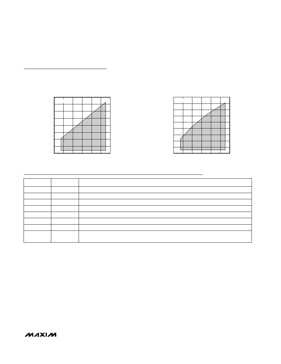
-0.5
1.5
0.5
4.5
3.5
2.5
7.5
6.5
5.5
8.5
2
4
3
5
6
7
8
MAX4198
INPUT COMMON-MODE RANGE vs.
SUPPLY VOLTAGE
MAX4198toc29
SUPPLY VOLTAGE (V)
INPUT COMMON-MODE VOLTAGE (V)
V
REF
= V
CC
/2
Pin Description
Feedback Resistor. Can be used as a sense input.
FB
5
Amplifier Output
OUT
6
Positive Supply Voltage
V
CC
7
Shutdown Control. Shutdown threshold is referenced to V
CC
. When pulled 2.5V below V
CC
, part
is in shutdown.
SHDN
8
Negative Supply Voltage
V
EE
4
Noninverting Input
IN+
3
PIN
Inverting Input
IN-
2
Reference Voltage Input. Offsets output voltage.
REF
1
FUNCTION
NAME