Applications information, Rail-to-rail output stage, Shutdown mode – Rainbow Electronics MAX4198_MAX4199 User Manual
Page 10: Driving capacitive loads, Power supply considerations, Application circuits
MAX4198/MAX4199
Rail-to-Rail Output Stage
The MAX4198/MAX4199 output stage incorporates a
common-source rail-to-rail structure which maximizes the
dynamic range of the differential amplifier. The output
can swing to within 100mV from each rail with a 5k
Ω
load
to V
CC
/ 2 (see
Typical Operating Characteristics
).
Shutdown Mode
The MAX4198/MAX4199 have an active-low shutdown
input. SHDN input logic thresholds are referenced to
V
CC
, not to GND. Pulling SHDN 2.5V below the positive
rail places the amplifiers in a 12µA (max) shutdown
mode. The MAX4198/MAX4199 exit or enter shutdown
in 35µs. In shutdown, the OUT pin is high-impedance.
Applications Information
Driving Capacitive Loads
The MAX4198/MAX4199 are relatively immune to oscilla-
tions caused when driving large capacitive loads.
Although heavy load capacitance increases transient ring-
ing, sustained oscillations typically don’t occur for loads
under 600pF (see Pulse Response with Capacitive Load
in the
Typical Operating Characteristics
). Applications that
require driving higher capacitive loads can isolate the out-
put capacitance using a 15
Ω
to 100
Ω
resistor between the
amplifier output and the load (Figure 1). Although adding
an isolation resistor dampens the response enough to pre-
vent oscillations, it does so at the expense of bandwidth
and DC accuracy.
Power Supply Considerations
The MAX4198/MAX4199 operate from single +2.7V to
+7.5V supplies or from dual ±1.35V to ±3.75V supplies,
and they consume only 45µA of supply current.
Excellent power-supply rejection permits the amplifiers
to be operated directly from a decaying 3V cell without
excessive error. To maximize AC performance, the sup-
ply must be bypassed with a 0.1µF ceramic capacitor
to ground that must be as close as possible to the pin.
If dual supplies are used, bypass both supply pins with
0.1µF to ground.
Application Circuits
Differential amplifiers can be used in single-ended and
other amplifier applications. Figures 2 through 6 show
the MAX4198/MAX4199 in different configurations. The
internally trimmed and matched resistors offer conven-
ience and have a distinct advantage over external
resistors. These amplifiers are not compensated for sin-
gle-ended unity gain; therefore, IN- should not be con-
nected to OUT or left unconnected.
Micropower, Single-Supply, Rail-to-Rail
Precision Differential Amplifiers
10
______________________________________________________________________________________
MAX4198
MAX4199
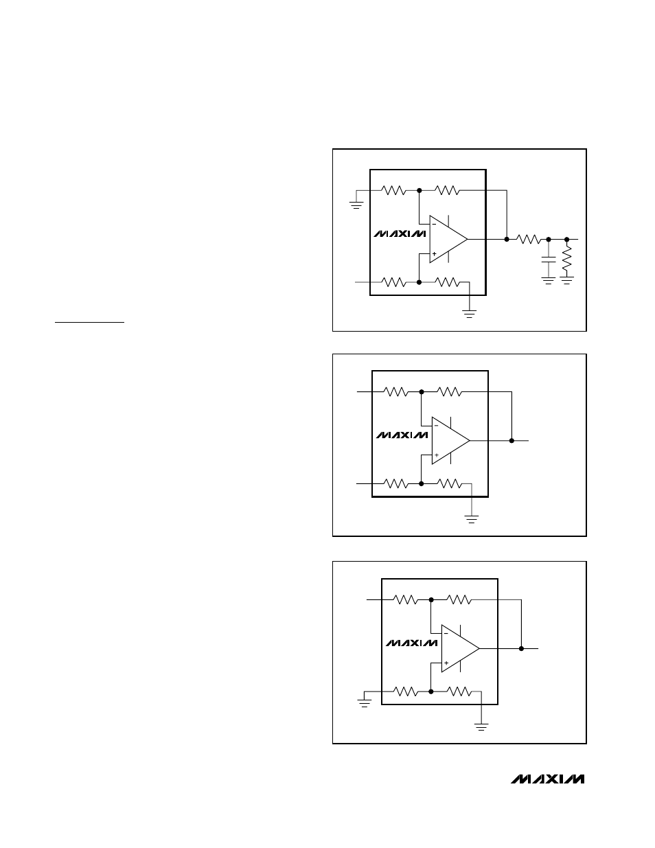
R
ISO
FB
OUT
V
EE
V
CC
INPUT
IN+
IN-
REF
C
L
R
L
OUTPUT
Figure 1. Dual-Supply, Capacitive-Load Driving Circuit
MAX4198
MAX4199
FB
OUT
V
EE
V
CC
IN+
IN-
V
A
V
B
REF
V
OUT
V
OUT
= (V
B
- V
A
)
(MAX4198)
V
OUT
= 10 (V
B
- V
A
)
(MAX4199)
Figure 2. Standard Difference Amplifier
MAX4198
MAX4199
FB
OUT
V
EE
V
CC
IN+
IN-
V
A
REF
V
OUT
V
OUT
= -V
A
(MAX4198)
V
OUT
= -10V
A
(MAX4199)
Figure 3. Precision Inverting Buffer