Electrical characteristics (max5259) – Rainbow Electronics MAX5259 User Manual
Page 4
MAX5258/MAX5259
+3V/+5V, Low-Power, 8-Bit Octal DAC
with Rail-to-Rail Output Buffers
4
_______________________________________________________________________________________
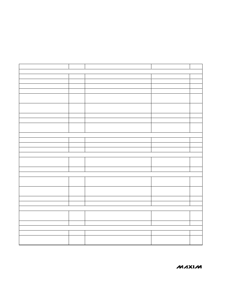
ELECTRICAL CHARACTERISTICS (MAX5259)
(V
DD
= +2.7V to +3.3V, V
REF
= +2.5V, GND = 0, R
L
= 10k
Ω, C
L
= 100pF, T
A
= T
MIN
to T
MAX
, unless otherwise noted. Typical values
are at V
DD
= +3V, and T
A
= +25°C.)
PARAMETER
SYMBOL
CONDITIONS
MIN
TYP
MAX
UNITS
STATIC ACCURACY
Resolution
8
Bits
Integral Non Linearity (Note 1)
INL
±0.1
±1
LSB
Differential Non Linearity (Note 1)
DNL
Guaranteed monotonic (all codes)
±0.1
±1
LSB
Zero-Code Error
ZCE
Code = 0A hex
±2.5
±20
mV
Zero-Code Error Supply
Rejection
Code = 0A hex.
0.15
1
LSB
Zero-Code Temperature
Coefficient
Code = 0A hex
±10
µV/
o
C
Full-Scale Error
Code = FF hex
±0.7
±30
mV
Full-Scale Error Supply Rejection
Code = FF hex
0.2
1
LSB
Full-Scale Temperature
Coefficient
Code = FF hex
±10
µV/
o
C
REFERENCE INPUTS
Input Voltage Range
0
V
DD
V
Input Resistance
161
218
300
k
Ω
Input Capacitance
20
pF
DAC OUTPUTS
Output Voltage Swing
R
L
= 10k
Ωto GND
0
V
DD
–
0.3
V
Output Voltage Range
R
L
= 10k
Ω to GND
0
V
REF
V
DIGITAL INPUTS
Input High Voltage
V
IH
0.7 x
V
DD
V
Input Low Voltage
V
IL
0.3 x
V
DD
V
Input Current
I
IN
V
IN
= 0 to V
DD
±1.0
µA
Input Capacitance
C
IN
(Note 3)
10
pF
DIGITAL OUTPUTS
Output High Voltage
V
OH
I
SOURCE
= 0.2mA
V
DD
–
0.5
V
Output Low Voltage
V
OL
I
SINK
= 1.6mA
0.4
V
DYNAMIC PERFORMANCE
Voltage-Output Slew Rate
Code = FF hex
0.55
V/
µs
Output Settling Time
To 1/2 LSB, from code 0A to code FF hex
(Note 2)
7
µs