Rainbow Electronics MAX5259 User Manual
Page 17
Power Sequencing
The voltage applied to REF should not exceed V
DD
at
any time. If proper power sequencing is not possible,
connect an external Schottky diode between REF and
V
DD
to ensure compliance with the absolute maximum
ratings. Do not apply signals to the digital inputs before
the device is fully powered-up.
Power-Supply Bypassing and
Ground Management
Bypass V
DD
with a 0.1µF capacitor, located as close to
V
DD
and GND as possible. Careful PC board layout
minimizes crosstalk among DAC outputs and digital
inputs. Figure 10 shows suggested circuit board layout
to minimize crosstalk.
Unipolar-Output, Two-Quadrant
Multiplication
In unipolar operation, the output voltages and the refer-
ence input are the same polarity. Figure 11 shows the
MAX5258/MAX5259 unipolar configuration, and Table 2
shows the unipolar code.
MAX5258/MAX5259
+3V/+5V, Low-Power, 8-Bit Octal DAC
with Rail-to-Rail Output Buffers
______________________________________________________________________________________
17
REF
R1
R15
R16
R255
R0
D7
D6
D5
D4
DAC A
MSB DECODER
D3
D0
D2
D1
LSB DECODER
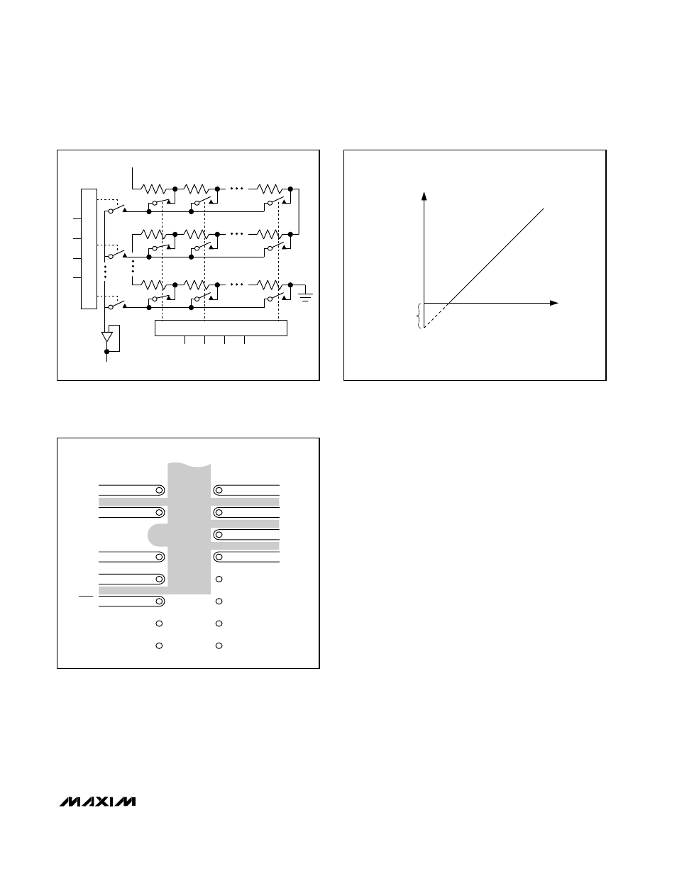
Figure 8. DAC Simplified Circuit Diagram
OUTC
OUTD
DOUT
DIN
SYSTEM GND
OUTB
OUTA
GND
V
DD
REF
LDAC
Figure 10. Suggested PC Board Layout for Minimizing
Crosstalk (Bottom View)
O
DAC CODE
NEGATIVE
OFFSET
OUTPUT
VOLTAGE
Figure 9. Effect of Negative Offset (Single Supply)