Pin description detailed description, Typical operating characteristics (continued) – Rainbow Electronics MAX7447 User Manual
Page 4
MAX7447
4-Channel S-Video, CVBS Video Filter with
Asynchronous CVBS Input
4
_______________________________________________________________________________________
Pin Description
Detailed Description
The MAX7447 filters and buffers video-encoder DAC
outputs in applications such as set-top boxes, hard-
disk recorders, DVD players, and digital VCRs. The
MAX7447 reconstructs and cleans up analog video sig-
nals from the output of DAC video encoders. Each
channel consists of a lowpass filter and an output video
buffer that drives two standard 150
Ω video loads.
The MAX7447 is designed to process S-Video and
CVBS video signals. The video signal processed by
channel A (CVBS video signal) must include a sync
pulse. This sync pulse provides the required timing for
channels A, B, and C. Channel D allows an asynchro-
nous CVBS video signal to be processed with its own
local sync separator.
This device operates from a single +5V supply and has
a nominal cutoff frequency of 5MHz optimized for
NTSC, PAL, and SDTV.
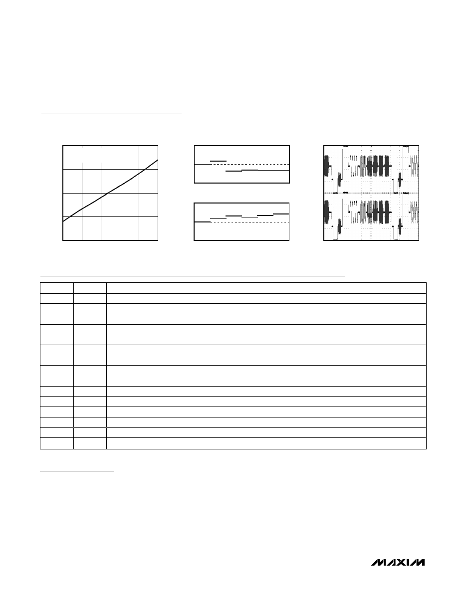
SUPPLY CURRENT vs. TEMPERATURE
MAX7447 toc07
TEMPERATURE (
°C)
SUPPLY CURRENT (mA)
60
35
10
-15
90
100
110
120
80
-40
85
INPUTS BIASED TO +2V
NO LOAD
DIFFERENTIAL GAIN
MAX7447 toc08
DIFFERENTIAL PHASE (DEGREES)
1st
3rd
2nd
4th
5th
6th
1st
3rd
2nd
4th
5th
6th
0.2
0.3
0.1
0
-0.1
-0.2
-0.3
DIFFERENTIAL GAIN (%)
0.2
0.3
0.1
0
-0.1
-0.2
-0.3
DIFFERENTIAL PHASE
MULTIBURST RESPONSE
MAX7447 toc09
10
µs/div
250mV/div
250mV/div
Typical Operating Characteristics (continued)
(V
CC
= +5V, T
A
= +25°C, unless otherwise noted.)
PIN
NAME
FUNCTION
1
INA
C hannel A V i d eo Inp ut. U se channel A for a C V BS video signal. AC - coup l e IN A w i th a ser i es 0.1µF cap aci tor .
2
INB
Channel B Video Input. Use channel B for the luma (Y) video signal. AC-couple INB with a series 0.1µF
capacitor.
3
INC
Channel C Video Input. Use channel C for the chroma (C) video signal. AC-couple INC with a series 0.1µF
capacitor.
4
IND
Channel D Video Input. Use channel D for a second CVBS video signal. AC-couple IND with a series 0.1µF
capacitor.
5
DISABLE
Disable Logic Input. A logic-low on DISABLE enables the output buffers. A logic-high on DISABLE disables
all output buffers and puts them in a high-impedance state.
6–9
GND
Ground
10
V
CC
+5V Supply Input
11
OUTD
Channel D Video Output. This output can be either AC- or DC-coupled.
12
OUTC
Channel C Video Output. This output can be either AC- or DC-coupled.
13
OUTB
Channel B Video Output. This output can be either AC- or DC-coupled.
14
OUTA
Channel A Video Output. This output can be either AC- or DC-coupled.