Pin description – Rainbow Electronics MAX8758 User Manual
Page 9
MAX8758
Step-Up Regulator with Switch Control and
Operational Amplifier for TFT LCD
_______________________________________________________________________________________
9
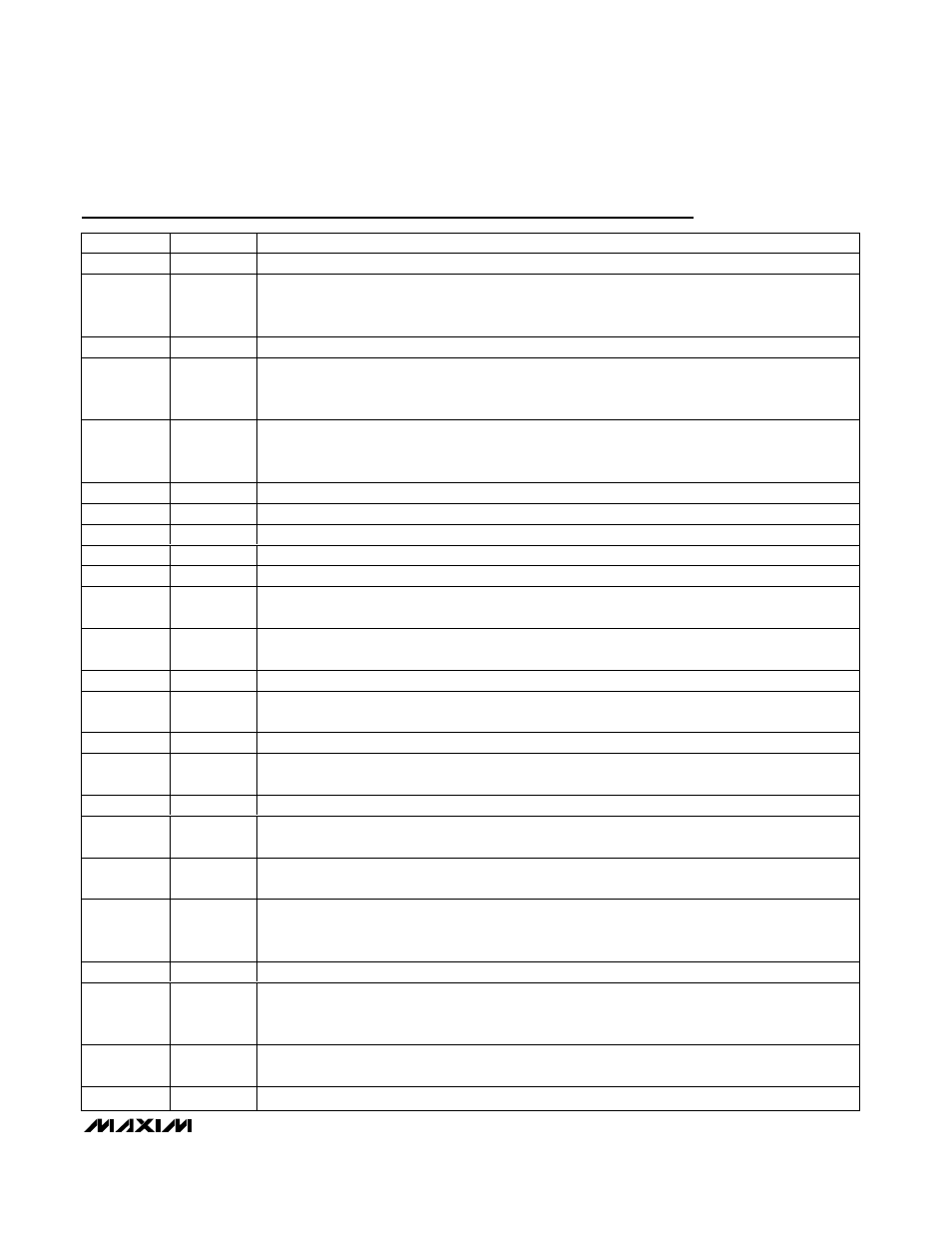
Pin Description
PIN
NAME
FUNCTION
1
GND
Analog Ground
2
GON
Internal High-Voltage-Switch Common Connection. GON is the output of the high-voltage-switch-
control block. GON is internally pulled to PGND through a 1k
Ω resistor in shutdown. See the High-
Voltage Switch Control section for details.
3
CTL
H i g h- V ol tag e, S w i tch- C ontr ol Bl ock Ti m i ng P i n. S ee the H i g h- V ol tag e S w i tch C ontr ol secti on for d etai l s.
4
DLP
High-Voltage, Switch-Control Block Delay Pin. Connect a capacitor from DLP to GND to set the delay
time. A 5µA current source charges C
DLP
. DLP is internally pulled to GND by a resistor in shutdown.
See the High-Voltage Switch Control section for details.
5
THR
GON Falling Regulation Adjustment Pin. Connect THR to the center of a resistive voltage-divider
between LDO or OUT and GND to adjust the V
GON
falling regulation level. The actual regulation level
is 10 x V
THR
. See the High-Voltage Switch Control section for details.
6
SUPB
Operational Amplifier Supply Input. Bypass SUPB to GND with a 0.1µF capacitor.
7
OUTB
Operational Amplifier Output
8
NEGB
Operational Amplifier Inverting Input
9
POSB
Operational Amplifier Noninverting Input
10
N.C.
No Connection. Not internally connected.
11
LDO
5V Internal Linear Regulator Output. This regulator powers all internal circuitry except the operational
amplifier. Bypass LDO to GND with a 0.22µF or greater ceramic capacitor.
12
OUT
Internal Linear Regulator Supply Pin. OUT is the supply input of the internal 5V linear regulator.
Connect OUT directly to the output of the step-up regulator.
13
I.C.
Internally Connected. Make no connection to this pin.
14
SS
Soft-Start Control Pin. Connect a capacitor between SS and GND to set the soft-start period of the
step-up regulator. See the Bootstrapping and Soft-Start section for details.
15
COMP
Error Amplifier Compensation Pin. See the Step-Up Regulator Loop Compensation section for details.
16
FREQ
Frequency-Select Pin. Connect FREQ to GND for 600kHz operation, and connect FREQ to IN for
1.2MHz operation.
17
IN
Supply Pin. Bypass IN to GND with a 1µF ceramic capacitor. Place the capacitor close to the IN pin.
18
LX
Switching Node. LX is the drain of the internal power MOSFET. Connect the inductor and the Schottky
diode to LX and minimize trace area for low EMI.
19
SHDN
Shutdown Control Pin. Pull
SHDN low to turn off the step-up regulator, the operational amplifier, and
the switch control block.
20
FB
Feedback Pin. The FB regulation point is 1.24V (typ). Connect FB to the center of a resistive voltage-
divider between the step-up regulator output and GND to set the step-up regulator output voltage.
Place the divider close to the FB pin.
21
PGND
Power Ground
22
MODE
High-Voltage, Switch-Control Block-Mode Selection Timing-Adjustment Pin. See the High-Voltage
Switch Control section for details. MODE is high impedance when it is connected to LDO. MODE is
internally pulled down by a 1k
Ω resistor during UVLO, when V
DLP
< 0.5 x V
LDO
, or in shutdown.
23
DRN
High-Voltage, Switch-Control Input. DRN is the drain of the internal high-voltage p-channel MOSFET
connected to GON.
24
SRC
High-Voltage Switch-Control Input. SRC is the source of the internal high-voltage p-channel MOSFET.