Rainbow Electronics MAX8758 User Manual
Page 2
MAX8758
Step-Up Regulator with Switch Control and
Operational Amplifier for TFT LCD
2
_______________________________________________________________________________________
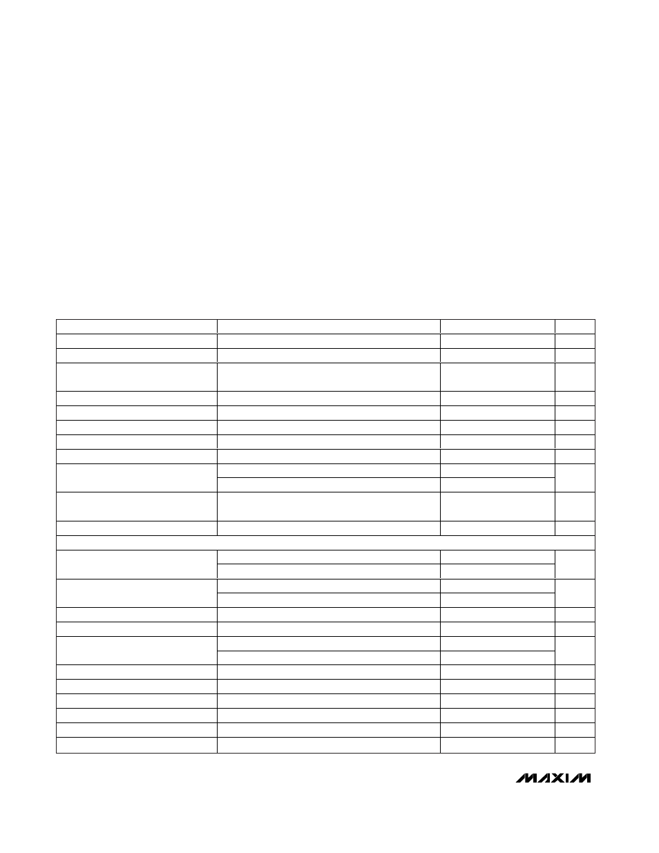
ABSOLUTE MAXIMUM RATINGS
ELECTRICAL CHARACTERISTICS
(V
IN
= V
SHDN
= +3V, OUT = +10V, FREQ = GND,
T
A
= 0°C to +85°C, unless otherwise noted. Typical values are at T
A
= +25°C.)
Stresses beyond those listed under “Absolute Maximum Ratings” may cause permanent damage to the device. These are stress ratings only, and functional
operation of the device at these or any other conditions beyond those indicated in the operational sections of the specifications is not implied. Exposure to
absolute maximum rating conditions for extended periods may affect device reliability.
IN,
SHDN, CTL, LDO to GND ...................................-0.3V to +6V
SUPB, LX, OUT to GND..........................................-0.3V to +14V
OUTB, NEGB, POSB to GND ..................-0.3V to (SUPB + 0.3V)
THR, DLP, MODE, FREQ, COMP, FB,
SS to GND..............................................-0.3V to VLDO + 0.3V
PGND to GND ......................................................-0.3V to + 0.3V
SRC to GND ..........................................................-0.3V to + 30V
GON, DRN to GND ....................................-0.3V to VSRC + 0.3V
GON RMS Current Rating................................................± 50mA
OUTB RMS Current Rating ..............................................± 60mA
LX RMS Current Rating .........................................................1.6A
Continuous Power Dissipation (TA = +70°C)
24-Pin, 4mm x 4mm Thin QFN
(derate 16.9mW/°C above +70°C) ..........................1349.1mW
Operating Temperature Range ...........................-40°C to +85°C
Junction Temperature ......................................................+150°C
Storage Temperature Range .............................-65°C to +160°C
Lead Temperature (soldering, 10s) .................................+300°C
PARAMETER
CONDITIONS
MIN
TYP
MAX
UNITS
IN Input Voltage Range
1.8
5.5
V
IN Quiescent Current
V
IN
= 3V, V
FB
= 1.5V
27
40
µA
IN Undervoltage Lockout
IN rising, 200mV hysteresis, LX remains off below
this level
1.3
1.75
V
LDO Output Voltage
6V
≤ V
OUT
≤ 13V, I
LDO
= 12.5mA, V
FB
= 1.5V (Note1)
4.8
5.0
5.2
V
LDO Undervoltage Lockout Voltage
LDO rising, 200mV hysteresis
2.4
2.7
3.0
V
OUT Supply Voltage Range
(Note 1)
4.5
13.0
V
OUT Overvoltage Fault Threshold
13.2
13.6
14.0
V
OUT Undervoltage Fault Threshold
1.4
V
V
FB
= 1.5V, no load
0.5
2.0
OUT Supply Current
V
FB
= 1.1V, no load
4
10.0
mA
Shutdown Supply Current
(Total of IN, OUT, and SUPB)
V
IN
= V
OUT
= V
SUPB
= 3V
4
10
µA
Thermal Shutdown
Temperature rising, 15°C hysteresis
+160
°C
STEP-UP REGULATOR
FREQ = GND
512
600
768
Operating Frequency
FREQ = IN
1020
1200
1380
kHz
FREQ = GND
91
95
99
Oscillator Maximum Duty Cycle
FREQ = IN
88
92
96
%
FB Regulation Voltage
1.228
1.24
1.252
V
FB Fault Trip Level
Falling edge
0.96
1.0
1.04
V
FREQ = GND
43
51
64
Duration to Trigger Fault Condition
FREQ = IN
47
55
65
ms
FB Load Regulation
0 < I
LOAD
< 200mA, transient only
-1
%
FB Line Regulation
V
IN
= 1.8V to 5.5V
-0.15
-0.08
+0.15
%/V
FB Input Bias Current
V
FB
= 1.3V
125
200
nA
FB Transconductance
∆I = 5µA at COMP
75
160
280
µS
FB Voltage Gain
FB to COMP
700
V/V
LX On-Resistance
I
LX
= 200mA
115
200
m
Ω