Pin description, Functional diagram – Rainbow Electronics MAX4987BE User Manual
Page 5
MAX4987AE/MAX4987BE
Overvoltage-Protection Controller
with USB ESD Protection
_______________________________________________________________________________________
5
Pin Description
PIN
NAME
FUNCTION
1
IN
Voltage Input. Bypass IN with a 1µF ceramic capacitor as close to the device as possible to obtain
±15kV HBM ESD protection. No capacitor required to obtain ±2kV HBM ESD protection.
2
CD+
USB Data Line
3
GND
Ground
4
CD-
USB Data Line
5
V
CC
Positive Supply-Voltage Input. V
CC
is required only when USB signals are present.
6
EN
Enable Active-Low Input. Drive
EN low to enable the switch. Drive EN high to disable the switch.
7
ACOK
Open-Drain Adapter-Voltage Indicator Output.
ACOK is driven low after the V
IN
voltage is stable
between UVLO and OVLO for 30ms (typ). Connect a pullup resistor from
ACOK to the logic I/O voltage
of the host system.
8
OUT
Output Voltage. Output of internal switch.
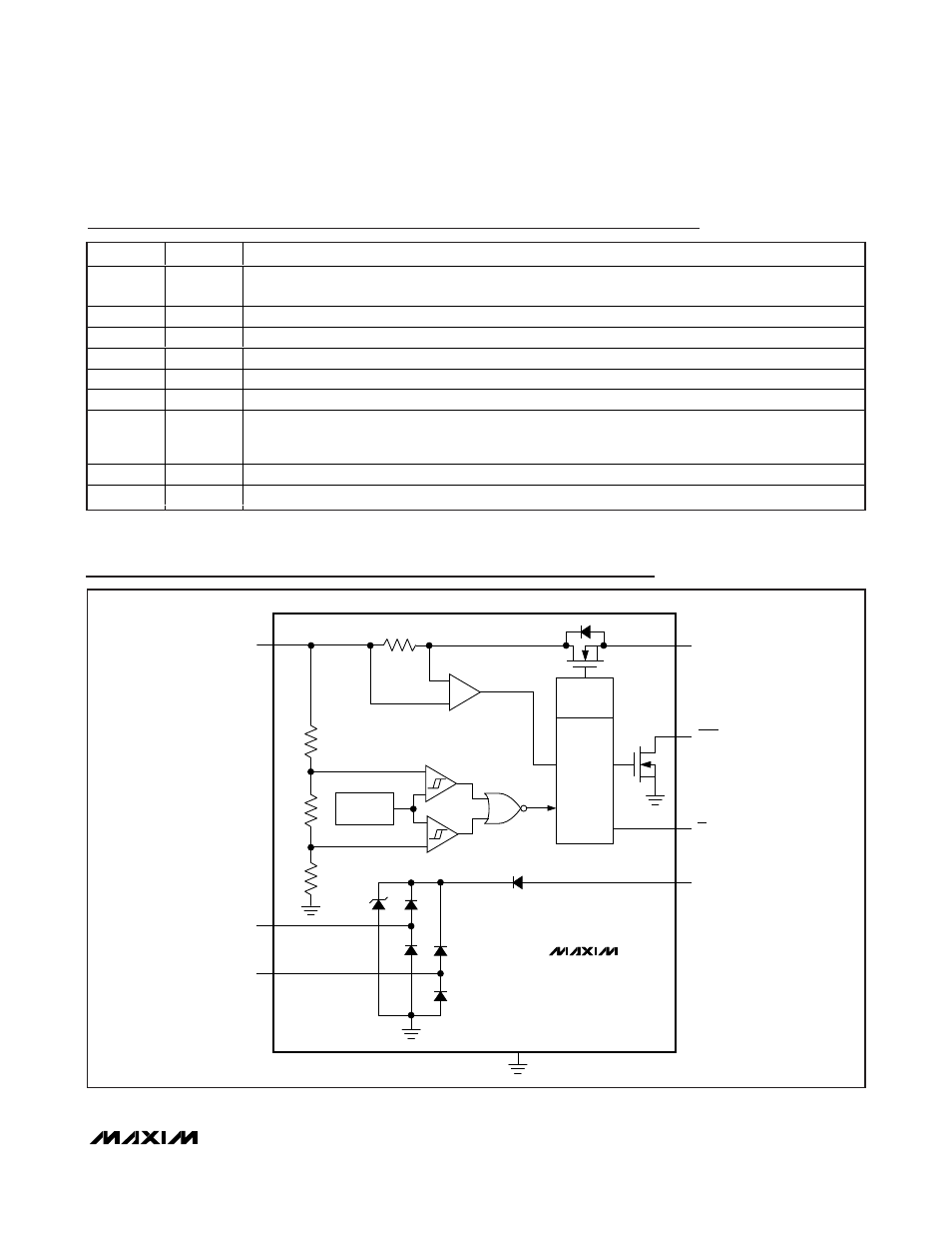
EP
EP
Exposed Pad. Connect exposed pad to ground. Do not use EP as a sole ground connection.
OVERCURRENT
FAULT
IN
CD+
CD-
V
CC
CHARGE
PUMP
CONTROL
LOGIC
MAX4987AE/
MAX4987BE
ACOK
V
BG
REFERENCE
+
-
+
-
OV
UV
EN
EN
OUT
GND
Functional Diagram