Rainbow Electronics MAX4987BE User Manual
Page 2
MAX4987AE/MAX4987BE
Overvoltage-Protection Controller
with USB ESD Protection
2
_______________________________________________________________________________________
ABSOLUTE MAXIMUM RATINGS
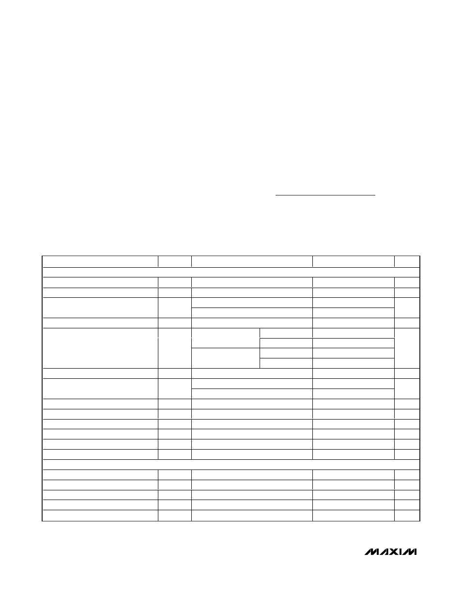
ELECTRICAL CHARACTERISTICS
(V
IN
= +2.2V to +28V, T
A
= -40°C to +85°C, unless otherwise noted. Typical values are at V
IN
= +5V and T
A
= +25°C.)
Stresses beyond those listed under “Absolute Maximum Ratings” may cause permanent damage to the device. These are stress ratings only, and functional
operation of the device at these or any other conditions beyond those indicated in the operational sections of the specifications is not implied. Exposure to
absolute maximum rating conditions for extended periods may affect device reliability.
(All voltages referenced to GND.)
IN ............................................................................-0.3V to +30V
OUT.............................................................-0.3V to +(IN + 0.3V)
V
CC
,
EN, ACOK, CD+, CD- ......................................-0.3V to +6V
Continuous Power Dissipation (T
A
= +70°C) for multilayer board:
8-Pin TDFN (derate 16.7mW/°C above +70°C) .........1333mW
Package Junction-to-Ambient Thermal Resistance
(
θ
JA
) (Note 1) ................................................................60.0°C/W
Package Junction-to-Case Thermal Resistance
(
θ
JC
) (Note 1) ................................................................10.8°C/W
Operating Temperature Range ...........................-40°C to +85°C
Junction Temperature ......................................................+150°C
Storage Temperature Range .............................-65°C to +150°C
Lead Temperature (soldering) .........................................+300°C
PARAMETER
SYMBOL
CONDITIONS
MIN
TYP
MAX
UNIT
ANALOG SWITCH
Input-Voltage Range
V
IN
2.2
28
V
V
CC
Input Voltage
V
CC
5.5
V
EN = 0V, V
IN
> V
UVLO
60
150
Input Supply Current
I
IN
EN = 5V, V
IN
> V
UVLO
50
100
µA
UVLO Supply Current
I
UVLO
V
IN
< V
UVLO
40
µA
MAX4987AE
2.3
(V
IN
falling)
MAX4987BE
3.8
MAX4987AE
2.35
2.55
2.75
IN Undervoltage Lockout
V
UVLO
(V
IN
rising)
MAX4987BE
3.85
4.2
4.45
V
IN Undervoltage Lockout Hysteresis
1
%
(V
IN
rising)
5.55
6.15
6.45
Overvoltage Trip Level
V
OVLO
(V
IN
falling)
5.5
V
IN Overvoltage Lockout Hysteresis
1
%
Switch On-Resistance
R
ON
V
IN
= 5V, I
OUT
= 500mA
100
200
m
Ω
Overcurrent Protection Threshold
I
LIM
1.5
4.2
A
Maximum Output Capacitance
V
IN
= 5V, no overcurrent shutdown
1000
µF
CD+ and CD- Leakage Current
I
LKG_CD
V
CC
= 5.5V, V
CD_
= 0V, 3.3V
-300
+300
nA
CD+ and CD- Capacitance
C
CD
f = 1MHz, V
CD_
= 0.5
P-P
3
pF
DIGITAL SIGNALS
ACOK Output Low Voltage
V
OL
I
SINK
= 1mA
0.4
V
ACOK High-Leakage Current
V
ACOK
= 5.5V, flag deasserted
1
µA
EN Input-Voltage High
V
IH
1.4
V
EN Input-Voltage Low
V
IL
0.4
V
EN Input-Leakage Current
I
LEAK
V
EN
= 5.5V
-1
+1
µA
Note 1: Package thermal resistances were obtained using the method described in JEDEC specification JESD51-7, using a 4-layer
board. For detailed information on package thermal considerations, go to www.maxim-ic.com/thermal-tutorial.