Electrical characteristics, Absolute maximum ratings – Rainbow Electronics MAX8815A User Manual
Page 2
MAX8815A
1A, 97% Efficiency, 30µA Quiescent Current
Step-Up Converter with True Shutdown
2
_______________________________________________________________________________________
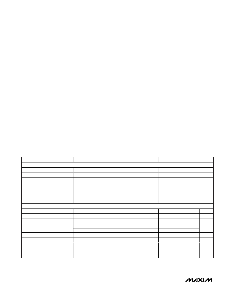
ELECTRICAL CHARACTERISTICS
(V
OUTS
= V
POUT
= 5V, V
ON
= V
BATT
= 3.6V, V
SKIPB
= GND, T
A
= -40°C to +85°C, typical values are at T
A
= +25°C, unless otherwise
noted. Limits are 100% production tested at T
A
= +25°C. Limits over the operating temperature range are guaranteed by design and
characterization.)
Stresses beyond those listed under “Absolute Maximum Ratings” may cause permanent damage to the device. These are stress ratings only, and functional
operation of the device at these or any other conditions beyond those indicated in the operational sections of the specifications is not implied. Exposure to
absolute maximum rating conditions for extended periods may affect device reliability.
PARAMETER
CONDITIONS
MIN
TYP
MAX
UNITS
GENERAL
Operating Input Voltage Range
1.2
5.5
V
Minimum Startup Voltage
1.2
1.5
V
T
A
= +25°C
0.1
1
Shutdown Supply Current
ON = GND
T
A
= +85°C
0.2
µA
No load, no switching, V
FB
= 1.28V
16
30
Supply Current
No load, switching (measured with external feedback);
V
POUT
= 5V
30
µA
OSCILLATOR
Switching Frequency
1.8
2.0
2.2
MHz
Maximum Duty Cycle
87.5
%
Output-Voltage Adjust Range
3.3
5.0
V
No load, T
A
= +25°C
1.255
1.265
1.275
FB Regulation Voltage
No load, T
A
= -40°C to +85°C (Note 3)
1.252
1.265
1.277
V
FB Load Regulation
-7.5
mV/A
FB Line Regulation
V
BATT
= 1.8V to 5V, I
POUT
= 0.5A
-10
mV/D
T
A
=+25°C
-50
-5
+50
FB Input Leakage Current
V
FB
= 1.28V, V
OUTS
=
V
POUT
= V
BATT
= 5.5V
T
A
= +85°C
-5
nA
Idle Mode™ Trip Level
(Note 4)
90
mA
ABSOLUTE MAXIMUM RATINGS
OUTS, BATT to GND ................................................-0.3V to +6V
POUT to OUTS ......................................................-0.3V to +0.3V
PGND (EP) to AGND .............................................-0.3V to +0.3V
FB to GND ................................................-0.3V to (V
OUT
+ 0.3V)
ON, SKIPB to GND ............-0.3V to the higher of (V
OUTS
+ 0.3V)
and (V
BATT
+ 0.3V)
LX Continuous Current (Note 1)..........................................2.75A
Continuous Power Dissipation (T
A
= +70°C)
10-Pin TDFN Single-Layer Board (derate 18.5 mW/°C
above +70°C)...........................................................1481.5mW
10-Pin TDFN Multilayer Board (derate 24.4 mW/°C
above +70°C)...........................................................1951.2mW
Junction-to-Case Thermal Resistance (
θ
JC
) (Note 2)
10-Pin TDFN .................................................................8.5°C/W
Junction-to-Ambient Thermal Resistance (
θ
JA
) (Note 2)
10-Pin TDFN ..................................................................41°C/W
Operating Temperature Range ...........................-40°C to +85°C
Junction Temperature Range ............................-40°C to +150°C
Storage Temperature Range .............................-65°C to +150°C
Lead Temperature (soldering, 10s) .................................+300°C
Note 1: LX has internal clamp diodes to PGND (EP) and VPWR, where VPWR is the internal power node and is the higher of BATT
and OUTS. Applications that forward bias these diodes should take care not to exceed the power-dissipation limits of the
device.
Note 2: Package thermal resistances were obtained using the method described in JEDEC specification JESD51-7, using a 4-layer
Idle Mode is a trademark of Maxim Integrated Products, Inc.