Chip information, Package information, Table 1. recommended inductors – Rainbow Electronics MAX8815A User Manual
Page 12
MAX8815A
1A, 97% Efficiency, 30µA Quiescent Current
Step-Up Converter with True Shutdown
Inductor Selection
In most step-up converter designs, a reasonable induc-
tor value can be derived from the following equation.
This equation sets peak-to-peak inductor current at 1/2
the DC inductor current:
L = (2 x V
BATT
x D x (1 - D))/(I
OUT(MAX)
x f
SW
)
where f
SW
is the switching frequency (2MHz), and D is
the duty factor given by D = 1 - (V
BATT
/V
OUT
). Using L
from the equation above results in a peak-to-peak
inductor current ripple of 0.5 x I
OUT
/(1 - D), and a peak
inductor current of 1.25 x I
OUT
/(1 - D). Ensure that the
peak (saturation) current rating of the inductor meets or
exceeds this requirement. The recommended induc-
tance range for the MAX8815A is 1µH to 2.2µH. See
Table 1 for recommended inductors.
Capacitor Selection
Output Capacitor
Output capacitor C2 in Figures 1a and 1b is required to
keep the output voltage ripple small and to ensure reg-
ulation loop stability. The output capacitors must have
low impedance at the switching frequency. Make sure
the output capacitors maintain their capacitance over
DC bias and the desired operating temperature range.
One 22µF tantalum capacitor is recommended.
Input Capacitor
Input capacitor C1 reduces the current peaks drawn
from the battery or input power source and reduce
switching noise in the IC. The impedance of the input
capacitor at the switching frequency should be kept
very low. A ceramic capacitor is highly recommended
due to their small size and low ESR. Make sure the
input capacitors maintain their capacitance over DC
bias and the desired operating temperature range.
Ceramic capacitors with X5R or X7R dielectric temper-
ature characteristics generally perform well. Two 4.7µF
or one 10µF ceramic capacitors are recommended.
PCB Layout and Routing
Good printed-circuit board (PCB) layout is important to
achieve optimal performance for the MAX8815A. Poor
design can cause excessive conducted and radiated
noise. Conductors carrying discontinuous currents and
any high-current path should be made as short and
wide as possible. Keep the feedback network (R1 and
R2) very close to the IC, preferably within 0.2in of the
FB and GND pins. Nodes with high dV/dt (switching
nodes) should be kept as small as possible and routed
away from FB. Connect the input and output capacitors
as close as possible to the IC. Refer to the MAX8815A
EV kit data sheet for a PCB layout example.
Chip Information
PROCESS: BiCMOS
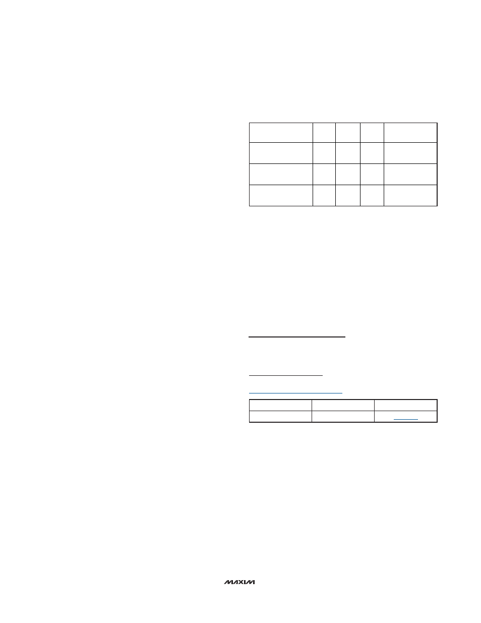
INDUCTOR
L
(µH)
DCR
(m
Ω)
I
SAT
(A)
SIZE (mm)
TOKO DE4012CK
A1101AS-1R0M
1
45
3.3
4 x 4 x 1.2
TOKO DE4012CK
A1101AS-2R2M
2.2
60
2.8
4 x 4 x 1.2
TOKO 2818C
1072AS-1R0M
1
40
2.8
2.8 x 2.8 x 1.8
Table 1. Recommended Inductors
PACKAGE TYPE
PACKAGE CODE
DOCUMENT NO.
10 TDFN-EP
T1033-2
Package Information
For the latest package outline information, go to
www.maxim-ic.com/packages
.
Maxim cannot assume responsibility for use of any circuitry other than circuitry entirely embodied in a Maxim product. No circuit patent licenses are
implied. Maxim reserves the right to change the circuitry and specifications without notice at any time.
12 ____________________Maxim Integrated Products, 120 San Gabriel Drive, Sunnyvale, CA 94086 408-737-7600
© 2008 Maxim Integrated Products
is a registered trademark of Maxim Integrated Products, Inc.