Electrical characteristics (continued) – Rainbow Electronics MAX5559 User Manual
Page 4
MAX5556–MAX5559
Low-Cost Stereo Audio DACs
4
________________________________________________________________________________________
ELECTRICAL CHARACTERISTICS (continued)
PARAMETER
SYMBOL
CONDITIONS
MIN
TYP
MAX
UNITS
INTERNAL SCLK MODE
LRCLK Duty Cycle
(Note 7)
50
%
Internal SCLK Period
t
ISCLK
(Note 8)
1 / f
SCLK
ns
LRCLK Edge to Internal SCLK
t
ISCLKR
t
ISCLK
/ 2
ns
SDATA Valid to Internal SCLK
t
ISDS
MCLK period = t
MCLK
t
MCLK
+ 10
ns
SDATA Valid to Internal SCLK
t
ISDH
MCLK period = t
MCLK
t
MCLK
ns
(V
DD
= +4.75V to +5.5V, GND = 0V, R
OUT
_ = 10kΩ, C
OUT
_ = 10pF, 0dBFS sine-wave signal at 997Hz, f
LRCLK
(f
S
) = 48kHz, f
MCLK
=
12.288MHz, measurement bandwidth 10Hz to 20kHz, unless otherwise specified. T
A
= -40°C to +85°C, unless otherwise noted.
Outputs are unloaded, unless otherwise noted. Typical values at V
DD
= +5V, T
A
= +25°C.) (Note 1)
Note 1: 100% production tested at T
A
= +85°C. Limits to -40°C are guaranteed by design.
Note 2: 0.5 LSB of triangular PDF dither added to data.
Note 3: Guaranteed by design, not production tested.
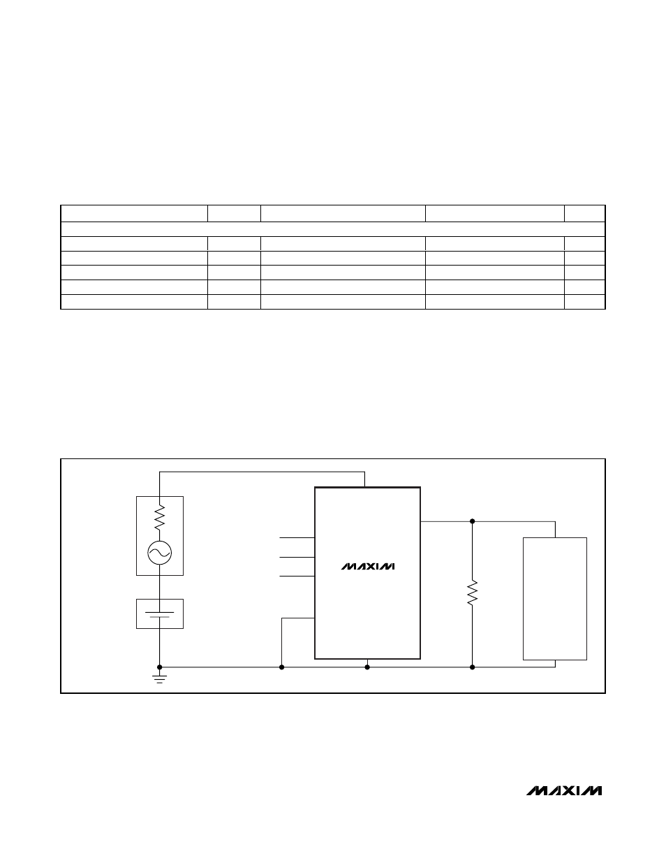
Note 4: PSRR test block diagram shown in Figure 1 denotes the test setup used to measure PSRR.
Note 5: Volume ramping interval starts from establishment of a valid MCLK to LRCLK ratio. Total time is proportional to the sample
rate (f
S
). 20ms based on 48ksps operation.
Note 6: In external SCLK mode, LRCLK duty cycles are not limited, provided all data formatting requirements are met. See Figures
4–7.
Note 7: The LRCLK duty cycle must be 50% ±1/2 MCLK period in internal SCLK mode.
Note 8: The SCLK/LRCLK ratio can be set to 32, 48, or 64, depending on the device and the MCLK/LRCLK ratio selected. See
Figures 4–7.
MCLK
SDATA
LRCLK
SCLK
ACTIVE CLOCKS
GND
V
DD
SPECTRUM
ANALYZER
LOUT, ROUT
Z
G
AUDIO SIGNAL
GENERATOR
(100mV
P-P
AT 1kHz)
DC POWER SUPPLY
(5VDC)
MAX5556–MAX5559
+
-
Figure 1. PSRR Test Block Diagram