Timing characteristics – Rainbow Electronics MAX5515 User Manual
Page 5
MAX5512–MAX5515
Dual, Ultra-Low-Power,
8-Bit, Voltage-Output DACs
_______________________________________________________________________________________
5
Note 1:
Linearity is tested within codes 6 to 255.
Note 2:
Offset is tested at code 6.
Note 3:
Gain is tested at code 255. For the MAX5514/MAX5515, FB_ is connected to its respective OUT_.
Note 4:
Guaranteed by design. Not production tested.
Note 5:
V
DD
must be a minimum of 1.8V.
Note 6:
Outputs can be shorted to V
DD
or GND indefinitely, provided that package power dissipation is not exceeded.
Note 7:
Optimal noise performance is at 2nF load capacitance.
Note 8:
Thermal hysteresis is defined as the change in the initial +25°C output voltage after cycling the device from T
MAX
to T
MIN
.
Note 9:
All digital inputs at V
DD
or GND.
Note 10:
Load = 10kΩ in parallel with 100pF, V
DD
= 5V, VREF = 4.096V (MAX5512/MAX5514) or V
REF
= 3.9V (MAX5513/MAX5515).
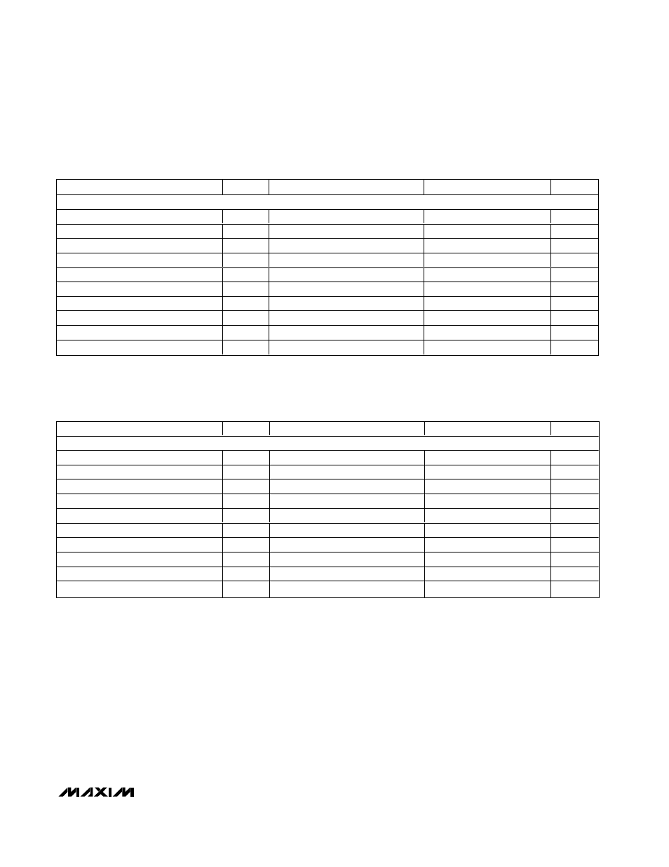
TIMING CHARACTERISTICS
(V
DD
= +4.5V to +5.5V, T
A
= T
MIN
to T
MAX
, unless otherwise noted. Typical values are at T
A
= +25°C.)
PARAMETER
SYMBOL
CONDITIONS
MIN
TYP
MAX
UNITS
TIMING CHARACTERISTICS (V
DD
= 4.5V to 5.5V )
Serial Clock Frequency
f
SCLK
0
16.7
MHz
DIN to SCLK Rise Setup Time
t
DS
15
ns
DIN to SCLK Rise Hold Time
t
DH
0
ns
SCLK Pulse-Width High
t
CH
24
ns
SCLK Pulse-Width Low
t
CL
24
ns
CS Pulse-Width High
t
CSW
100
ns
SCLK Rise to
CS Rise Hold Time
t
CSH
0
ns
CS Fall to SCLK Rise Setup Time
t
CSS
20
ns
SCLK Fall to
CS Fall Setup
t
CSO
0
ns
CS Rise to SCK Rise Hold Time
t
CS1
20
ns
TIMING CHARACTERISTICS
(VDD = +1.8V to +5.5V, TA = TMIN to TMAX, unless otherwise noted. Typical values are at TA = +25°C.)
PARAMETER
SYMBOL
CONDITIONS
MIN
TYP
MAX
UNITS
TIMING CHARACTERISTICS (V
DD
= 1.8V to 5.5V )
Serial Clock Frequency
f
SCLK
0
10
MHz
DIN to SCLK Rise Setup Time
t
DS
24
ns
DIN to SCLK Rise Hold Time
t
DH
0
ns
SCLK Pulse-Width High
t
CH
40
ns
SCLK Pulse-Width Low
t
CL
40
ns
CS Pulse-Width High
t
CSW
150
ns
SCLK Rise to
CS Rise Hold Time
t
CSH
0
ns
CS Fall to SCLK Rise Setup Time
t
CSS
30
ns
SCLK Fall to
CS Fall Setup
t
CSO
0
ns
CS Rise to SCK Rise Hold Time
t
CS1
30
ns