Detailed description, Functional diagrams (continued) – Rainbow Electronics MAX5515 User Manual
Page 13
Detailed Description
The MAX5512–MAX5515 dual, 8-bit, ultra-low-power,
voltage-output DACs offer Rail-to-Rail buffered voltage
outputs. The DACs operate from a 1.8V to 5.5V supply
and require only 5µA (max) supply current. These
devices feature a shutdown mode that reduces overall
current, including the reference input current, to just
0.18µA (max). The MAX5513/MAX5515 include an inter-
nal reference that saves additional board space and can
source up to 8mA, making it functional as a system refer-
ence. The 16MHz, 3-wire serial interface is compatible
with SPI, QSPI, and MICROWIRE protocols. When V
DD
is
applied, all DAC outputs are driven to zero scale with vir-
tually no output glitch. The MAX5512/MAX5513 output
buffers are configured in unity gain and come in µMAX
packages. The MAX5514/MAX5515 output buffers are
configured in force sense allowing users to externally set
voltage gains on the output (an output-amplifier inverting
input is available). The MAX5514/MAX5515 come in
4mm x 4mm thin QFN packages.
Digital Interface
The MAX5512–MAX5515 use a 3-wire serial interface
that is compatible with SPI/QSPI/MICROWIRE protocols
(Figures 1 and 2).
The MAX5512–MAX5515 include a single, 16-bit, input
shift register. Data loads into the shift register through
the serial interface. CS must remain low until all 16 bits
are clocked in. The 16 bits consist of 4 control bits
(C3–C0), 8 data bits (D7–D0) (
Table
1), and 4 sub-bits
(S3–S0). The sub-bits must be set to zero for proper
operation. Following the 4 control bits, the data loads
MSB first, D7–D0. D7–D0 are the DAC data bits and
S3–S0 are the sub-bits. The control bits C3–C0 control
the MAX5512–MAX5515, as outlined in
Table
2.
Each DAC channel includes two registers: an input reg-
ister and a DAC register. The input register holds input
data. The DAC register contains the data updated to
the DAC output.
The double-buffered register configuration allows any
of the following:
• Loading the input registers without updating the DAC
registers
• Updating the DAC registers from the input registers
• Updating all the input and DAC registers simultaneously
MAX5512–MAX5515
Dual, Ultra-Low-Power,
8-Bit, Voltage-Output DACs
______________________________________________________________________________________
13
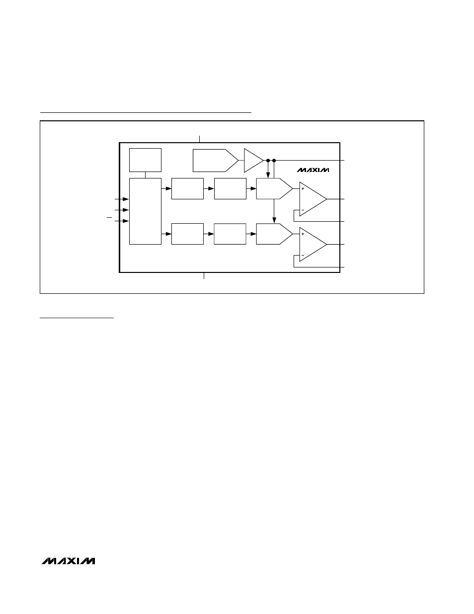
Functional Diagrams (continued)
8-BIT DAC
2-BIT
PROGRAMMABLE
REFERENCE
DAC
REGISTER
OUTA
REF
BUF
GND
MAX5515
REFOUT
INPUT
REGISTER
POWER-
DOWN
CONTROL
CONTROL
LOGIC
AND
SHIFT
REGISTER
8-BIT DAC
DAC
REGISTER
OUTB
FBA
FBB
SCLK
V
DD
DIN
CS
INPUT
REGISTER