Rainbow Electronics MAX4249_MAX4257 User Manual
Page 2

MAX4249–MAX4257
UCSP, Single-Supply, Low-Noise,
Low-Distortion, Rail-to-Rail Op Amps
2
_______________________________________________________________________________________
ABSOLUTE MAXIMUM RATINGS
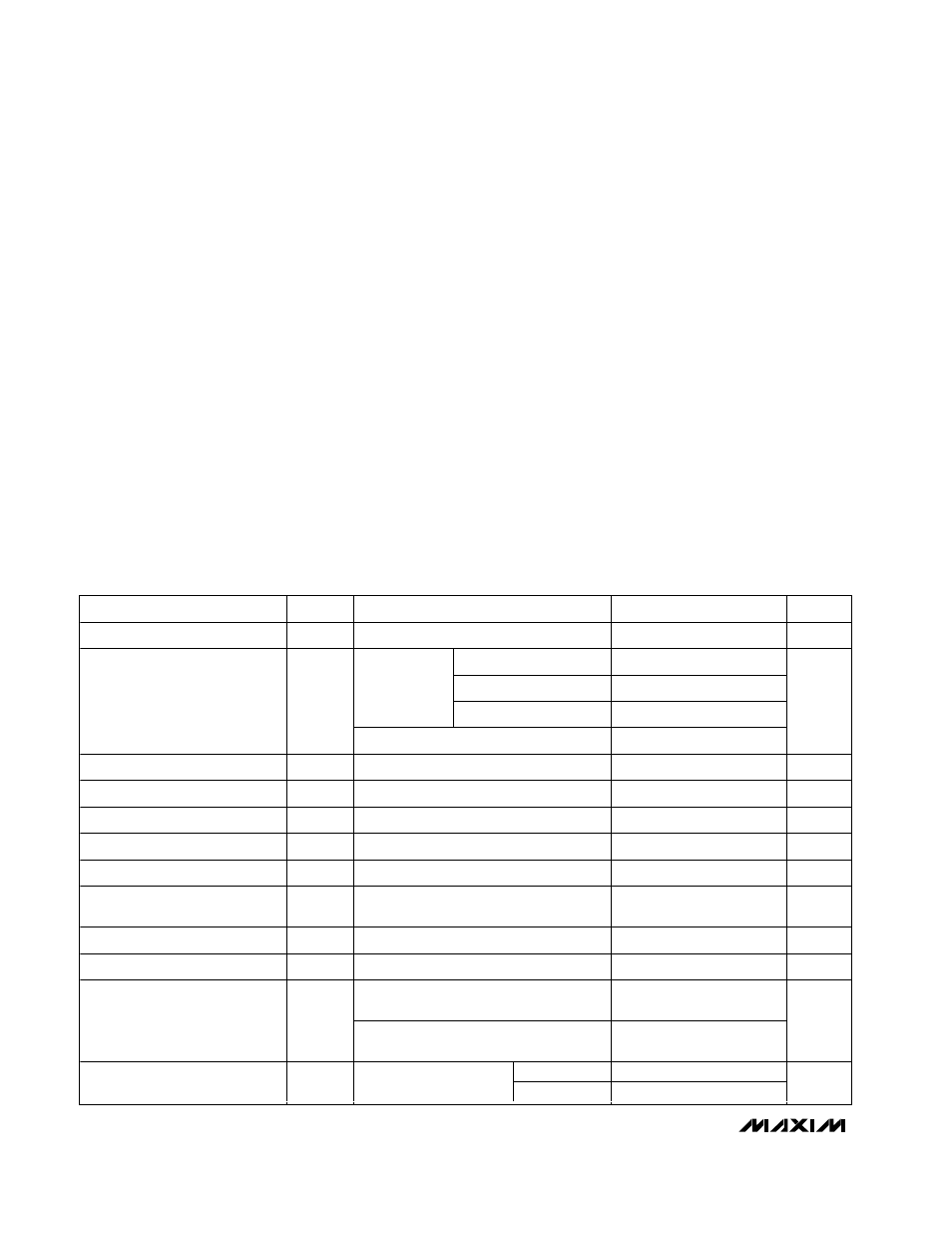
ELECTRICAL CHARACTERISTICS
(V
DD
= 5V, V
SS
= 0, V
CM
= 0, V
OUT
= V
DD
/2, R
L
tied to V
DD
/2, SHDN = V
DD
, T
A
= -40°C to +85°C, unless otherwise noted. Typical
values are at T
A
= +25°C.) (Notes 2, 3)
Stresses beyond those listed under “Absolute Maximum Ratings” may cause permanent damage to the device. These are stress ratings only, and functional
operation of the device at these or any other conditions beyond those indicated in the operational sections of the specifications is not implied. Exposure to
absolute maximum rating conditions for extended periods may affect device reliability.
Power-Supply Voltage (V
DD
to V
SS
) ......................+6.0V to -0.3V
Analog Input Voltage (IN_+, IN_-)....(V
DD
+ 0.3V) to (V
SS
- 0.3V)
SHDN Input Voltage ......................................6.0V to (V
SS
- 0.3V)
Output Short-Circuit Duration to Either Supply ..........Continuous
Continuous Power Dissipation (T
A
= +70°C)
5-Pin SOT23 (derate 7.1mW/°C above +70°C)...........571mW
8-Pin µMAX (derate 4.5mW/°C above +70°C) ............362mW
8-Pin SO (derate 5.88mW/°C above +70°C)...............471mW
8-Pin UCSP (derate 4.7mW/°C above +70°C) ............379mW
10-Pin UCSP (derate 6.1mW/°C above +70°C) ...........484mW
10-Pin µMAX (derate 5.6mW/°C above +70°C) ...........444mW
14-Pin SO (derate 8.33mW/°C above +70°C)..............667mW
Operating Temperature Range ...........................-40°C to +85°C
Junction Temperature ......................................................+150°C
Storage Temperature Range .............................-65°C to +150°C
Lead Temperature (soldering, 10s) .................................+300°C
Bump Temperature (soldering) (Note 1)
Infrared (15s) ................................................................+220°C
Vapor Phase (60s) ........................................................+215°C
PARAMETER
SYMBOL
CONDITIONS
MIN
TYP
MAX
UNITS
Supply Voltage Range
V
DD
(Note 4)
2.4
5.5
V
V
DD
= 3V
400
V
DD
= 5V
420
575
Normal mode
V
DD
= 5V, UCSP only
420
655
Quiescent Supply Current Per
Amplifier
I
Q
Shutdown mode (SHDN = V
SS
) (Note 2)
0.5
1.5
µA
Input Offset Voltage (Note 5)
V
OS
±0.07
±0.75
mV
Input Offset Voltage Tempco
TCV
OS
0.3
µV/°C
Input Bias Current
I
B
(Note 6)
±1
±100
pA
Input Offset Current
I
OS
(Note 6)
±1
±100
pA
Differential Input Resistance
R
IN
1000
G
Ω
Input Common-Mode Voltage
Range
V
CM
Guaranteed by CMRR test
-0.2
V
DD
- 1.1
V
Common-Mode Rejection Ratio
CMRR
V
SS
- 0.2V
≤ V
CM
≤ V
DD
- 1.1V
70
115
dB
Power-Supply Rejection Ratio
PSRR
V
DD
= 2.4 to 5.5V
75
100
dB
R
L
= 10k
Ω to V
DD
/2;
V
OUT
= 25mV to V
DD
- 4.97V
80
116
Large-Signal Voltage Gain
A
V
R
L
= 1k
Ω to V
DD
/2;
V
OUT
= 150V to V
DD
- 4.75V
80
112
dB
V
DD
- V
OH
8
25
Output Voltage Swing
V
OUT
|V
IN+
- V
IN-
|
≥ 10mV
R
L
= 10k
Ω to V
DD
/2
V
OL
- V
SS
7
20
mV
Note 1:
This device is constructed using a unique set of packaging techniques that impose a limit on the thermal profile the device
can be exposed to during board-level solder attach and rework. This limit permits only the use of the solder profiles rec-
ommended in the industry-standard specification, JEDEC 020A, paragrah 7.6, Table 3 for IR/VPR and Convection Reflow.
Preheating is required. Hand or wave soldering is not allowed.
