Pin description – Rainbow Electronics MAX15023 User Manual
Page 9
MAX15023
Wide 4.5V to 28V Input, Dual-Output
Synchronous Buck Controller
_______________________________________________________________________________________
9
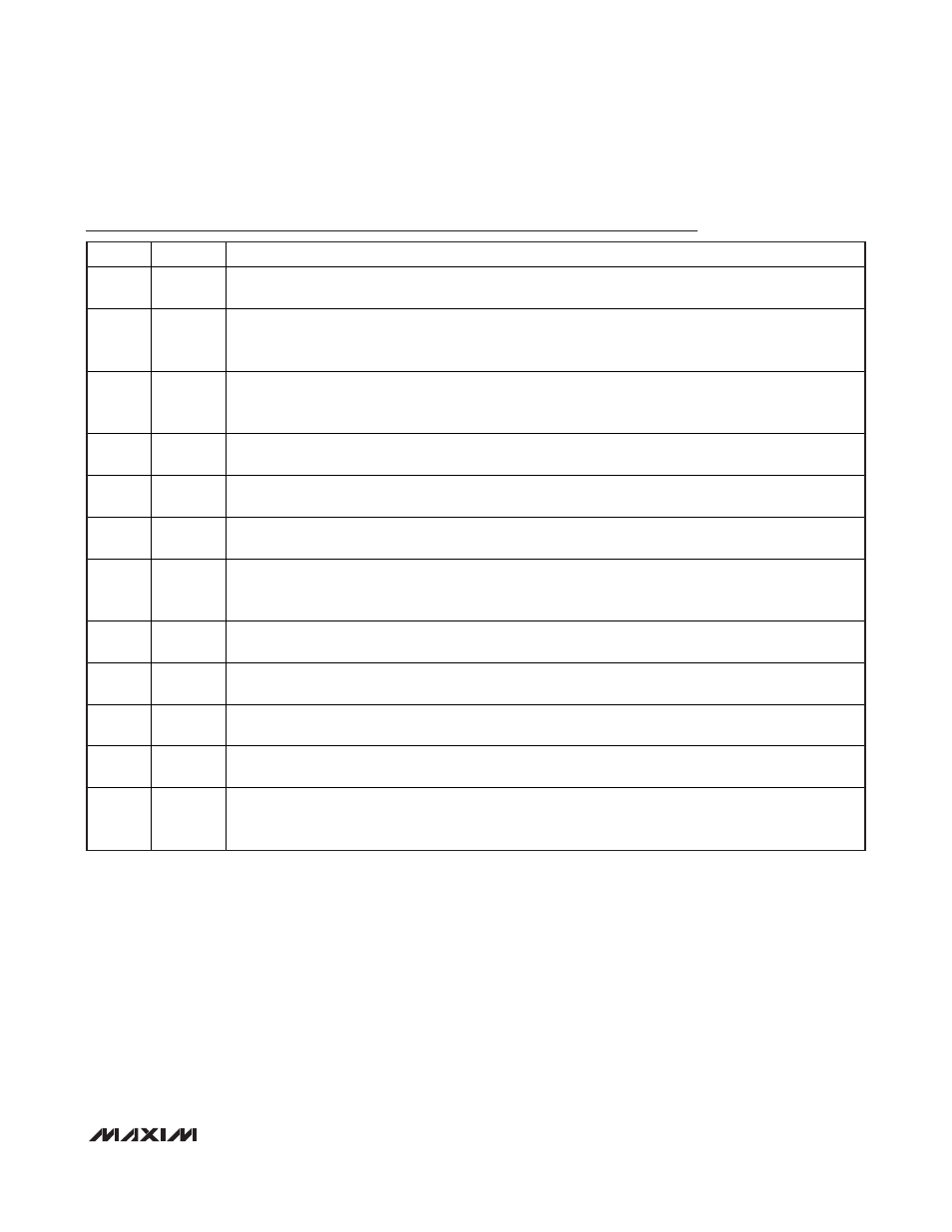
Pin Description
PIN
NAME
FUNCTION
1
FB1
Feedback Input for Regulator 1. Connect FB1 to a resistive divider between Output 1 and SGND to adjust
the output voltage between 0.6V and (0.85 x input voltage (V)). See the Setting the Output Voltage section.
2
EN1
Active-High Enable Input for Regulator 1. When the voltage at EN1 exceeds 1.2V (typ), the controller begins
regulating OUT1. When the voltage falls below 1.05V (typ), the regulator is turned off. The EN1 input can be
used for power sequencing and as a secondary UVLO. Connect EN1 to V
CC
for always-on applications.
3
EN2
Active-High Enable Input for Regulator 2. When the voltage at EN2 exceeds 1.2V (typ), the controller begins
regulating OUT2. When the voltage falls below 1.05V (typ), the regulator is turned off. The EN2 input can be
used for power sequencing and as a secondary UVLO. Connect EN2 to V
CC
for always-on applications.
4
PGOOD1
Power-Good Output (Open Drain) for Channel 1. To obtain a logic signal, pull up PGOOD1 with an external
resistor connected to a positive voltage below 28V.
5
DL1
Low-Side Gate-Driver Output for Regulator 1. DL1 swings from V
CC
to PGND1. DL1 is low before V
CC
reaches the UVLO rising threshold voltage.
6
PGND1
Low-Side Gate-Driver Supply Return (Regulator 1). Connect to the source of the low-side MOSFET of
Regulator 1.
7
LX1
External Inductor Connection for Regulator 1. Connect LX1 to the switched side of the inductor. LX1 serves
as the lower supply rail for the DH1 high-side gate driver and as sensing input of the synchronous
MOSFET’s V
DS
drop (drain terminal).
8
BST1
Boost Flying-Capacitor Connection for Regulator 1. Connect a ceramic capacitor with a minimum value of
100nF between BST1 and LX1.
9
DH1
High-Side Gate-Driver Output for Regulator 1. DH1 swings from LX1 to BST1. DH1 is low before V
CC
reaches the UVLO rising threshold voltage.
10
DH2
High-Side Gate-Driver Output for Regulator 2. DH2 swings from LX2 to BST2. DH2 is low before V
CC
reaches the UVLO rising threshold voltage.
11
BST2
Boost Flying-Capacitor Connection for Regulator 2. Connect a ceramic capacitor with a minimum value of
100nF between BST2 and LX2.
12
LX2
External Inductor Connection for Regulator 2. Connect LX2 to the switched side of the inductor. LX2 serves
as the lower supply rail for the DH2 high-side gate driver and as sensing input of the synchronous
MOSFET’s V
DS
drop (drain terminal).