Rainbow Electronics MAX15023 User Manual
Page 20
MAX15023
Wide 4.5V to 28V Input, Dual-Output
Synchronous Buck Controller
20
______________________________________________________________________________________
It is recommended to have a phase margin around
+50° to +60° to maintain a robust loop stability and
well-behaved transient response.
If an electrolytic or large-ESR tantalum output capacitor
is used, the capacitor ESR zero f
ZO
typically occurs
between the LC poles and the crossover frequency f
O
(f
PO
< f
ZO
< f
O
). In this case, use a Type II (PI or pro-
portional-integral) compensation network.
If a ceramic or low-ESR tantalum output capacitor is
used, the capacitor ESR zero typically occurs above
the desired crossover frequency f
O
, that is f
PO
< f
O
<
f
ZO
. In this situation, choose a Type III (PID or propor-
tional-integral-derivative) compensation network.
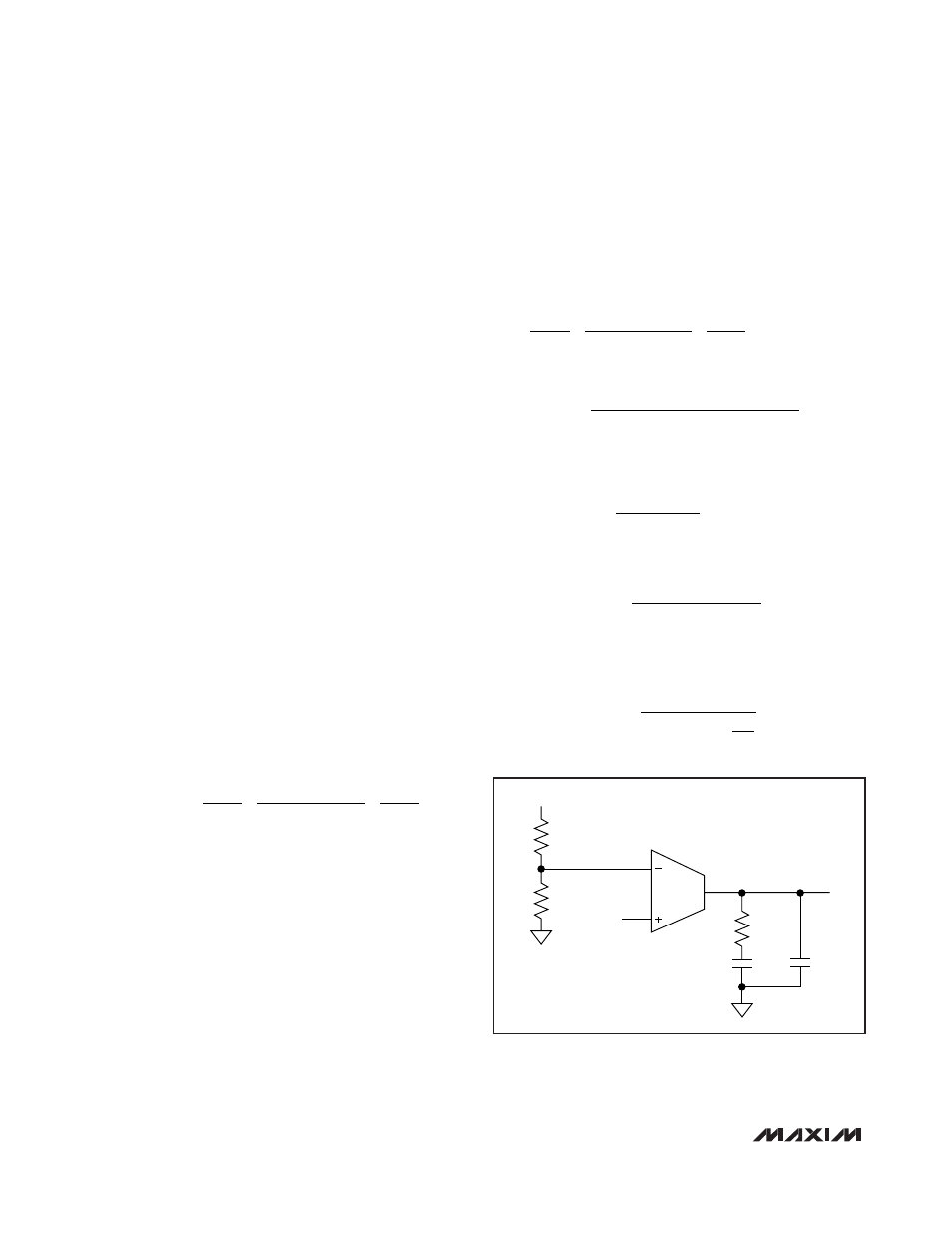
Type II Compensation Network
(See Figure 4)
If f
ZO
is lower than f
O
and close to f
PO
, the phase lead
of the capacitor ESR zero almost cancels the phase
loss of one of the complex poles of the LC filter around
the crossover frequency. Therefore, a Type II compen-
sation network with a midband zero and a high-fre-
quency pole can be used to stabilize the loop. In Figure
4, R
F
and C
F
introduce a midband zero (f
Z1
). R
F
and
C
CF
in the Type II compensation network also provide a
high-frequency pole (f
P1
), which mitigates the effects of
the output high-frequency ripple.
To calculate the component values for Type II compen-
sation network in Figure 4, follow the instruction below:
1) Calculate the gain of the modulator (Gain
MOD
)—
composed of the regulator’s pulse-width modulator,
LC filter, feedback divider, and associated circuitry
at crossover frequency:
where V
IN
is the regulator’s input voltage, V
OSC
is the
amplitude of the ramp in the pulse-width modulator,
V
FB
is the FB_ input voltage set-point (0.6V typically,
see
Electrical Characteristics
table), and V
OUT
is the
desired output voltage.
The gain of the error amplifier (Gain
EA
) in midband fre-
quencies is:
where g
m
is the transconductance of the error amplifier.
The total loop gain as the product of the modulator gain
and the error amplifier gain at f
O
should equal 1. So:
Therefore:
Solving for R
F
:
2) Set a midband zero (f
Z1
) at 0.75 x f
PO
(to cancel
one of the LC poles):
Solving for C
F
:
3) Place a high-frequency pole at f
P1
= 0.5 x f
SW
(to
attenuate the ripple at the switching frequency, f
SW
)
and calculate C
CF
using the following equation:
C
R
f
C
CF
F
SW
F
=
Ч
Ч
−
1
1
π
C
R
f
F
F
PO
=
Ч
Ч
Ч
1
2
0 75
π
.
f
R
C
f
Z
F
F
PO
1
1
2
0 75
=
Ч
Ч
=
Ч
π
.
R
V
f
L
V
V
V
g
ESR
F
OSC
O
OUT
OUT
FB
IN
m
=
Ч
Ч
Ч
(
)
Ч
Ч
Ч
Ч
2
π
V
V
ESR
f
L
V
V
g
R
IN
OSC
O
OUT
FB
OUT
m
F
Ч
Ч
Ч
Ч
Ч
Ч
=
(
)
2
1
π
Gain
Gain
MOD
EA
×
= 1
Gain
g
R
EA
m
F
=
×
Gain
V
V
ESR
f
L
V
V
MOD
IN
OSC
O
OUT
FB
OUT
=
Ч
Ч
Ч
(
)
Ч
2
π
V
REF
R
1
V
OUT
R
2
g
m
R
F
COMP
C
F
C
CF
Figure 4. Type II Compensation Network