Pin description (continued) – Rainbow Electronics MAX15023 User Manual
Page 10
MAX15023
Wide 4.5V to 28V Input, Dual-Output
Synchronous Buck Controller
10
______________________________________________________________________________________
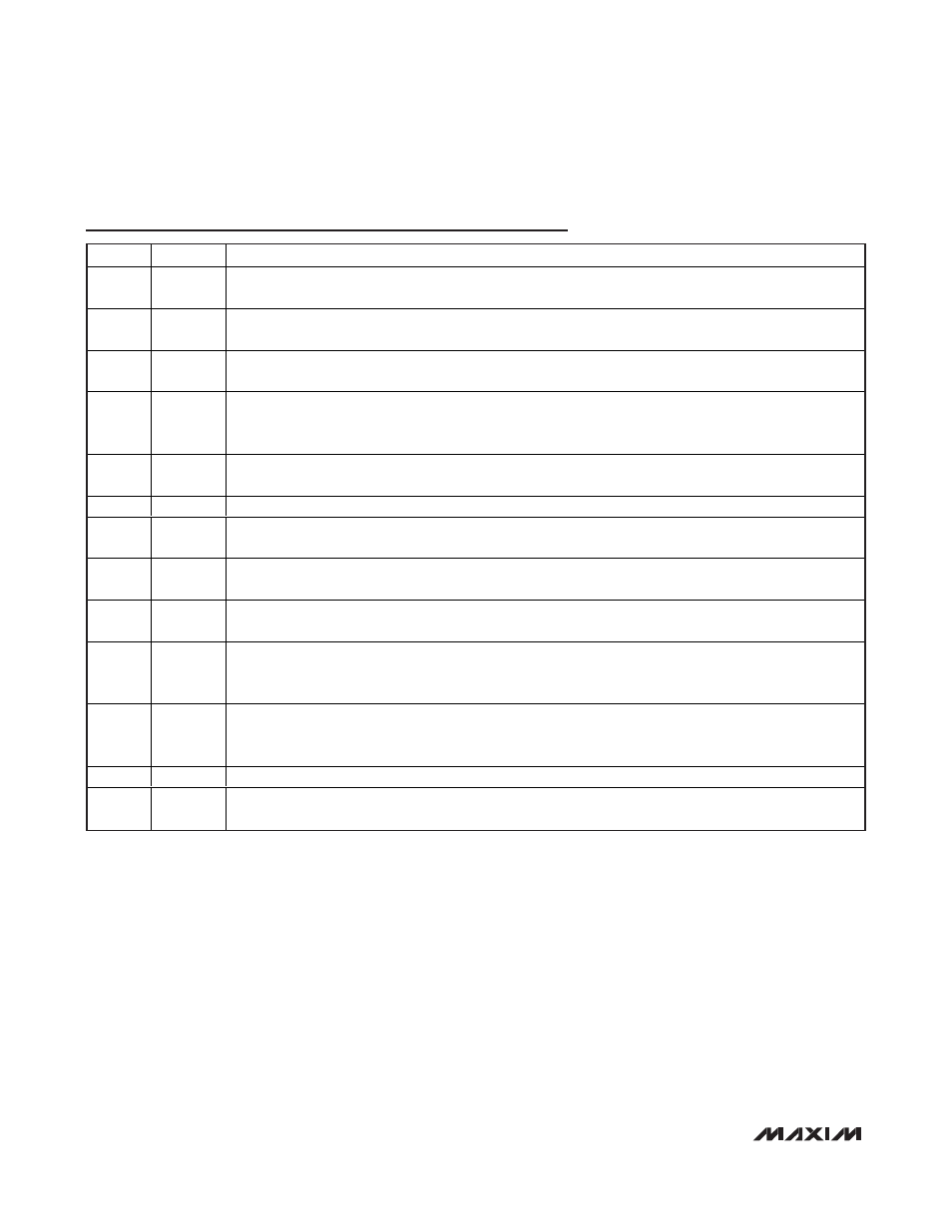
Pin Description (continued)
PIN
NAME
FUNCTION
13
PGND2
Low-Side Gate-Driver Supply Return (Regulator 2). Connect to the source of the low-side MOSFET of
Regulator 2.
14
DL2
Low-Side Gate-Driver Output for Regulator 2. DL2 swings from V
CC
to PGND2. DL2 is low before V
CC
reaches the UVLO rising threshold voltage.
15
PGOOD2
Power-Good Output (Open Drain) for Channel 2. To obtain a logic signal, pull up PGOOD2 with an external
resistor connected to a positive voltage below 28V.
16
V
CC
Internal 5.2V Linear Regulator Output and the Device’s Core Supply. When using the internal regulator,
bypass V
CC
to SGND with a 4.7µF minimum low-ESR ceramic capacitor. If V
CC
is connected to IN for 5V
operation, then a 2.2µF ceramic capacitor is adequate for decoupling (see the Typical Application Circuits).
17
FB2
Feedback Input for Regulator 2. Connect FB2 to a resistive divider between output 2 and SGND to adjust
the output voltage between 0.6V and (0.85 x input voltage (V)). See the Setting the Output Voltage section.
18
COMP2
Compensation Pin for Regulator 2. See the Compensation section.
19
RT
Oscillator-Timing Resistor Input. Connect a resistor from RT to SGND to set the oscillator frequency from
200kHz to 1MHz (see the Setting the Switching Frequency section).
20
SGND
Signal Ground. Connect SGND to the SGND plane. SGND also serves as sensing input of the synchronous
MOSFET’s V
DS
drop (source terminals) for both channels.
21
IN
Internal V
CC
Regulator Input. Bypass IN to SGND with a 1µF minimum ceramic capacitor when the
internal
linear regulator (V
CC
) is used. When operating in the 5V ±10% range, connect IN to V
CC
.
22
LIM2
Current-Limit Adjustment for Regulator 2. Connect a resistor (R
LIM2
) from LIM2 to SGND to adjust the
current-limit threshold (V
ITH2
) from 30mV (R
LIM2
= 6k
Ω) to 300mV (R
LIM2
= 60k
Ω). See the Setting the
Cycle-by-Cycle Low-Side Source Peak Current Limit section.
23
LIM1
Current-Limit Adjustment for Regulator 1. Connect a resistor (R
LIM1
) from LIM1 to SGND to adjust the
current-limit threshold (V
ITH1
) from 30mV (R
LIM1
= 6k
Ω) to 300mV (R
LIM1
= 60k
Ω). See the Setting the
Cycle-by-Cycle Low-Side Source Peak Current Limit section.
24
COMP1
Compensation Pin for Regulator 1. See the Compensation section.
—
EP
Exposed Paddle. Connect EP to a large copper plane at SGND potential to improve thermal dissipation. Do
not use as the main IC’s SGND ground connection.