Electrical characteristics, Absolute maximum ratings – Rainbow Electronics MAX9109 User Manual
Page 2
MAX9107/MAX9108/MAX9109
25ns, Dual/Quad/Single, Low-Power,
TTL Comparators
2
_______________________________________________________________________________________
Power-Supply Ranges
Supply Voltage (V
CC
to GND) ..............................................6V
Differential Input Voltage ........................-0.3V to (V
CC
+ 0.3V)
Common-Mode Input Voltage to GND ...-0.3V to (V
CC
+ 0.3V)
Latch-Enable Input Voltage
(MAX9109 only) ...................................-0.3V to (V
CC
+ 0.3V)
Output Short-Circuit Duration to V
CC
or GND ........................10s
Continuous Power Dissipation (T
A
= +70°C)
6-Pin SC70 (derate 3.1mW/°C above +70°C) ..............245mW
6-Pin SOT23 (derate 8.7mW/°C above +70°C)............696mW
8-Pin SOT23 (derate 9.1mW/°C above +70°C)............727mW
8-Pin SO (derate 5.9mW/°C above +70°C)..................470mW
14-Pin TSSOP (derate 9.1mW/°C above +70°C) .........727mW
14-Pin SO (derate 8.33mW/°C above +70°C)..............666mW
Operating Temperature Range ...........................-40°C to +85°C
Storage Temperature Range .............................-65°C to +150°C
Lead Temperature (soldering, 10s) .................................+300°C
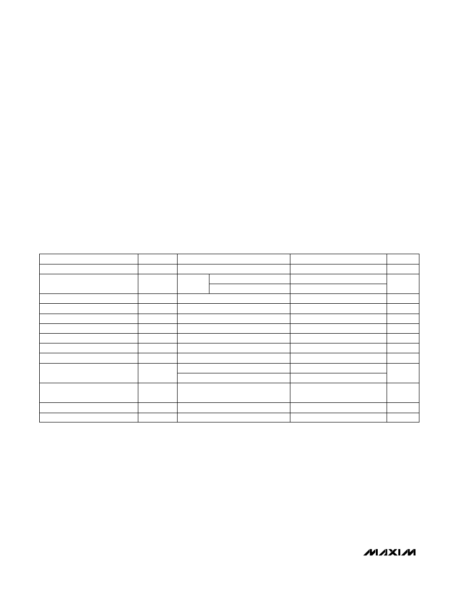
ELECTRICAL CHARACTERISTICS
(V
CC
= +5V, V
CM
= 0, V
LE
= 0 (MAX9109 only), T
A
= T
MIN
to T
MAX
, unless otherwise noted. Typical values are at T
A
= +25°C.) (Note 1)
Stresses beyond those listed under “Absolute Maximum Ratings" may cause permanent damage to the device. These are stress ratings only, and functional
operation of the device at these or any other conditions beyond those indicated in the operational sections of the specifications is not implied. Exposure to
absolute maximum rating conditions for extended periods may affect device reliability.
ABSOLUTE MAXIMUM RATINGS
PARAMETER
Operating Voltage Range
Input Bias Current
Input Offset Current
Common-Mode Rejection Ratio
Power-Supply Rejection Ratio
Output High Voltage
Output Low Voltage
Output Rise Time
Output Fall Time
t
f
t
r
V
OL
V
OH
PSRR
CMRR
I
OS
I
B
V
CC
SYMBOL
V
OUT
= 2.4V to 0.4V, C
L
= 10pF
V
OUT
= 0.4V to 2.4V, C
L
= 10pF
I
SINK
= 8mA
I
SINK
= 3.2mA
I
SOURCE
= 100µA
4.5V
≤ V
CC
≤ 5.5V
V
CC
= 5.5V (Note 5)
T
A
= +25
°C
Guaranteed by PSRR
CONDITIONS
MIN
TYP
MAX
4.5
5.5
0.5
1.6
125
350
25
80
50
1000
50
1000
3.0
3.5
0.35
0.6
0.4
12
6
ns
ns
V
V
µV/V
µV/V
nA
nA
V
UNITS
Input Hysteresis
V
HYST
(Note 3)
2
mV
Input Voltage Range
V
CMR
(Note 4)
-0.2
V
CC
- 1.5
V
mA
Supply Current Per Comparator
V
CC
= +5.5V, all outputs low
I
CC
0.35
0.7
Input Offset Voltage
V
OS
T
A
= T
MIN
to T
MAX
4.0
mV
(Note 2)