Applications information – Rainbow Electronics MAX8712 User Manual
Page 21

Charge-Pump Output Capacitor
Increasing the output capacitance or decreasing the
ESR reduces the output ripple voltage and the peak-to-
peak transient voltage. With ceramic capacitors, the
output voltage ripple is dominated by the capacitance
value. Use the following equation to approximate the
required capacitor value:
where C
OUT_CP
is the output capacitor of the charge
pump, I
LOAD_CP
is the load current of the charge
pump, and V
RIPPLE_CP
is the desired peak-to-peak
value of the output ripple.
Charge-Pump Rectifier Diode
Use low-cost silicon switching diodes with a current rat-
ing equal to or greater than two times the average
charge-pump input current. If it helps avoid an extra
stage, some or all of the diodes can be replaced with
Schottky diodes with an equivalent current rating.
Applications Information
External Transistor for Higher Current
or Power Dissipation
The load current and the voltage difference between
the input and output determine the linear regulator’s
power dissipation as shown in the following equation:
P
DISSIPATION
= (V
INL
- V
OUTL
) x I
OUTL
For some applications, the input voltage to the linear
regulator is from a 19V adapter. To make a 10V output,
the voltage across the pass transistor is 9V. In this case,
the regulator’s power dissipation may exceed the dissi-
pation limit that the package can handle. In some other
applications, the load current may be much higher than
the regulator’s guaranteed 300mA output current.
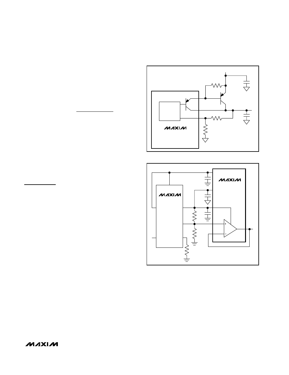
The solution for such applications is to connect an exter-
nal PNP transistor with the internal PNP transistor in a
Darlington configuration as shown in Figure 7. The
external pass transistor must be able to handle most of
the power dissipation since most of the load current
flows through it. On the other hand, the power dissipat-
ed in the internal pass transistor is very low. The current-
limit circuit will not work if an external pass transistor is
used because the linear regulator only senses the cur-
rent of the internal pass transistor.
Using the MAX1512 VCOM Calibrator
to Adjust the Buffer Output
The operational amplifier is typically used as the VCOM
buffer in TFT LCD panels. The output voltage of the
VCOM buffer can be adjusted using the MAX1512,
which is an EEPROM-programmable VCOM calibrator,
using the circuit shown in Figure 8. Refer to the
MAX1512 data sheet for details.
C
I
f
V
OUT CP
LOAD CP
OSC RIPPLE CP
_
_
_
≥
2
MAX8710/MAX8711/MAX8712
Low-Cost Linear-Regulator
LCD Panel Power Supplies
______________________________________________________________________________________
21
MAX8710
MAX8711
MAX8712
LINEAR
REGULATOR
4.7µF
4.7µF
INL
OUTL
FBL
V
IN
= 19V
KSB834W
(FAIRCHILD)
AVDD = 10V
51Ω
140kΩ
20kΩ
Figure 7. High-Power Linear Regulator
MAX8710
MAX8711
REF
V
DD
GND
OUTL
CE
AVDD
OUT
SET
CTL
OUTB
TO
VCOM
SUPB
POSB
NEGB
20kΩ
0.47µF
4.7µF
0.1µF
100kΩ
25kΩ
MAX1512
Figure 8. Using the MAX1512 to Adjust the VCOM Buffer Output
