Rainbow Electronics MAX8712 User Manual
Page 13

MAX8710/MAX8711/MAX8712
Low-Cost Linear-Regulator
LCD Panel Power Supplies
______________________________________________________________________________________
13
MMBD4148SE
(FAIRCHILD)
MMBD4148
2x MMBD4148SE
(FAIRCHILD)
0.22µF
0.47µF
1µF
R5
110kΩ
1%
R6
100kΩ
1%
DRVN
FBN
OUTL
AVDD
10V/300mA
GON
27V/20mA
GND
GND
IN
10.8V TO 13.2V
IN
0.1µF
10µF
4.7µF
1µF
0.1µF
R3
325kΩ
1%
0.1µF
0.1µF
C1
47pF
R2
33.2kΩ
1%
R4
33.2kΩ
1%
R1
100kΩ
1%
GOFF
-5V/50mA
REF
5V/1mA
SHDN
MAX8712
INL
REF
DLP
SHDN
FBP
DRVP
FBL
1µF
0.1µF
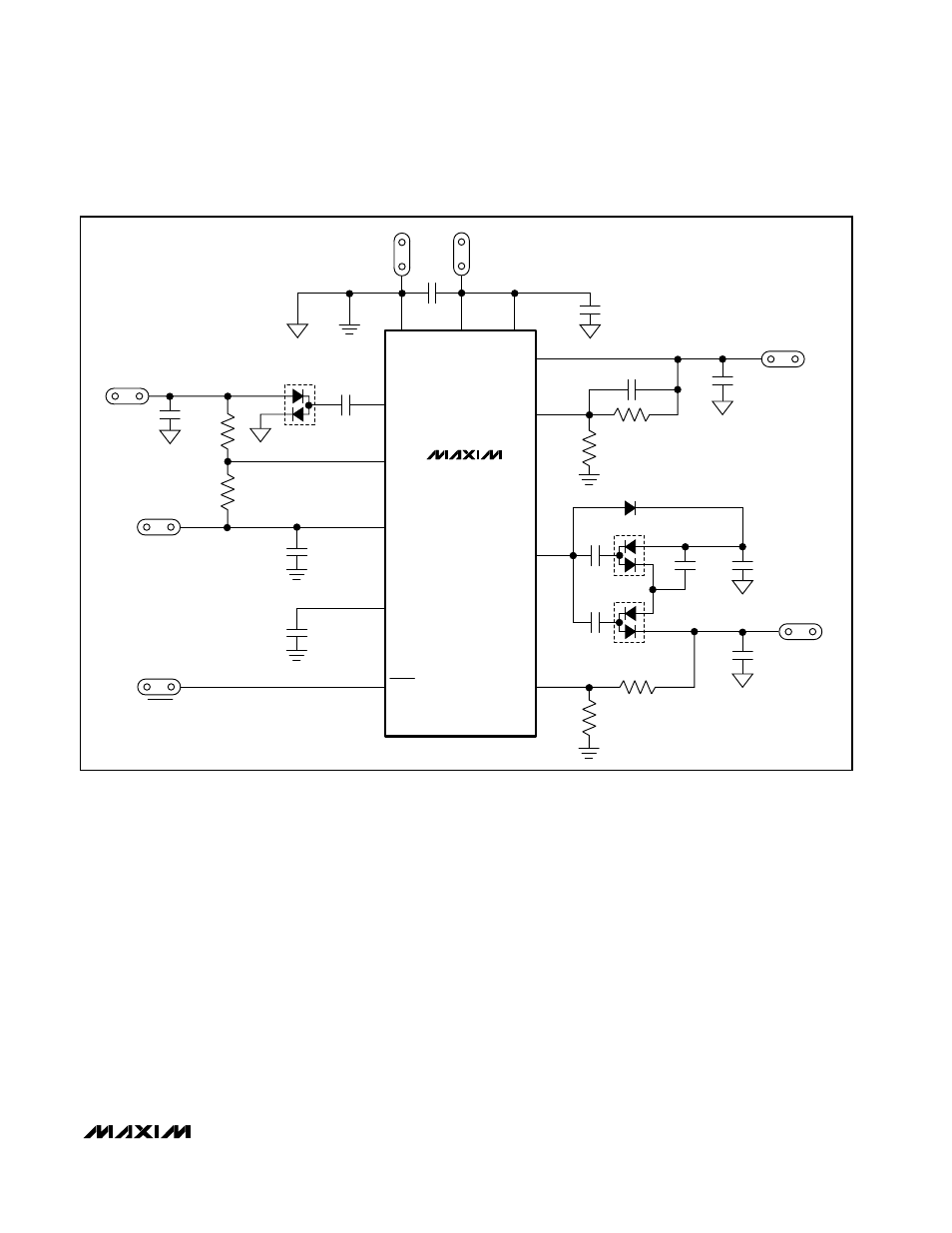
Figure 3. Typical Operating Circuit of the MAX8712
reference voltage, the controller lowers the base current
of the PNP transistor, which reduces the amount of cur-
rent delivered to the output. If the feedback voltage is too
low, the device increases the PNP transistor’s base cur-
rent, which allows more current to pass to the output and
raises the output voltage. The linear regulator also
includes an output current limit that protects the internal
pass transistor against short circuits.
The input voltage range of the linear regulator is from 8V
to 28V. The Typical Operating Circuits shown use a 12V
input. The output voltage range of the linear regulator
(OUTL) is up to 28V (MAX8710) or up to 14V
(MAX8711/MAX8712). The linear-regulator output is used
to generate the AVDD voltage, which is the analog supply
rail for source-driver ICs in TFT LCD panels. The typical
load of the AVDD supply is a periodic pulsed load, with a
peak current of approximately 1A and pulse width of
approximately 2µs. The period of the pulse load is
between 8.9µs and 31.7µs. The excellent transient perfor-
mance of the linear regulator can easily meet this tran-
sient-response requirement.
The linear regulator can deliver at least 300mA output
current continuously with a 4.7µF output capacitor. Do not
allow the device power dissipation to exceed the pack-
age-dissipation limit listed in the Absolute Maximum
Ratings section. The power dissipation can be estimated
by multiplying the voltage difference between the input
and the output with the required maximum continuous
output current. For applications where the power dissipa-
tion exceeds the package limit, see the External
Transistor for Higher Current or Power Dissipation section
for more information.
The linear regulator is enabled whenever REF is in regula-
tion and SHDN is logic high. Each time it is enabled, the
