Rainbow Electronics MAX8712 User Manual
Page 15

MAX8710/MAX8711/MAX8712
Low-Cost Linear-Regulator
LCD Panel Power Supplies
______________________________________________________________________________________
15
REF
V
SUPCP
FBN
250mV
0.5 x V
REF
SUPCP
DRVN
V
NEG
C
OUT(NEG)
C
X(NEG)
D3
D4
C
X(POS)
V
SUPCP
V
POS
C
OUT(POS)
D2
D1
DRVP
FBP
P2
N2
P1
N1
SEQUENCE
OSCILLATOR
MAX8710
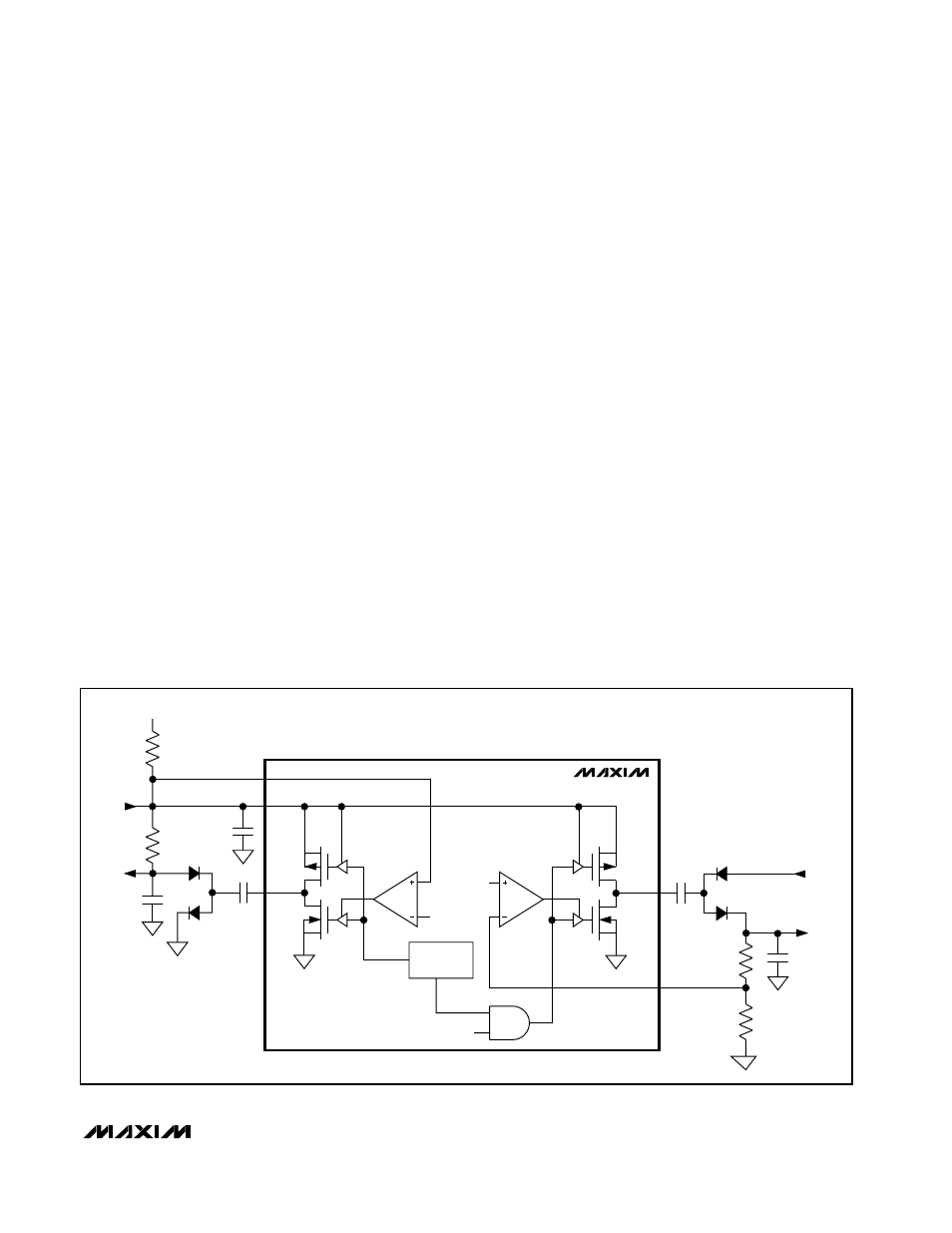
Figure 5. Charge-Pump Regulator Functional Diagram
linear regulator goes through a soft-start routine by ramp-
ing up its internal reference voltage from 0 to 2.5V in 128
steps. The soft-start period is 2.73ms (typ), and FBL fault
detection is disabled during this period. This soft-start
feature effectively limits the inrush current during startup.
The linear-regulator current-limit circuitry monitors the
current flowing through the internal pass transistor. The
internal current limit is approximately 800mA. The linear-
regulator output declines when it is not able to supply the
load current. If the FBL voltage drops below 0.75V, the
current limit folds back to approximately 100mA.
The MAX8710/MAX8711/MAX8712 monitor the FBL volt-
age for undervoltage conditions. If V
FBL
is continuously
below 2V (typ) for approximately 44ms, the device latch-
es off. The foldback current-limit circuit, in conjunction
with the output undervoltage fault latch and thermal-over-
load protection, protects the output load and the internal
pass transistor against short circuits or overloads.
Positive Charge-Pump Regulator
The positive charge-pump regulator is typically used to
generate the positive supply rail for the TFT LCD gate-dri-
ver ICs. The output voltage is set with an external resistive
voltage-divider from its output to GND with the midpoint
connected to FBP. The number of charge-pump stages
and the setting of the feedback divider determine the out-
put voltage of the positive charge-pump regulator. The
charge pump includes a high-side P-channel MOSFET
(P1) and a low-side N-channel MOSFET (N1) to control
the power transfer as shown in Figure 5. The MOSFETs
switch at a constant frequency of 1.5MHz.
During the first half-cycle, N1 turns on and allows V
INPUT
(V
SUPCP
, MAX8710 or VOUTL, MAX8711/MAX8712) to
charge up the flying capacitor C
X(POS)
through diode
D1. The amount of charge transferred from V
INPUT
to
C
X(POS)
is determined by the on-resistance of N1, which
varies according to the output of the feedback error
amplifier. The error amplifier compares the feedback sig-
nal (FBP) with a 2.5V internal reference and amplifies the
difference. If the feedback signal is below the reference,
the error-amplifier output increases the supply voltage of
N1’s gate driver, lowering the on-resistance. Similarly, if
the feedback signal is above the reference, the error-
amplifier output reduces the driver supply voltage,
increasing the on-resistance. During the second half-
cycle, N1 turns off and P1 turns on, level shifting C
X(POS)
by V
INPUT
volts. This connects C
X(POS)
in parallel with
the reservoir capacitor C
OUT(POS)
. If the voltage
across C
OUT(POS)
plus a diode drop (V
POS
+ V
DIODE
) is
smaller than the level-shifted flying-capacitor voltage
