Unipolar output, Bipolar output, Gain error – Rainbow Electronics MAX5133 User Manual
Page 15: Settling time, Digital feedthrough
MAX5132/MAX5133
+5V/+3V, 13-Bit, Serial, Force/Sense DACs
with 10ppm/°C Internal Reference
______________________________________________________________________________________
15
Gain Error
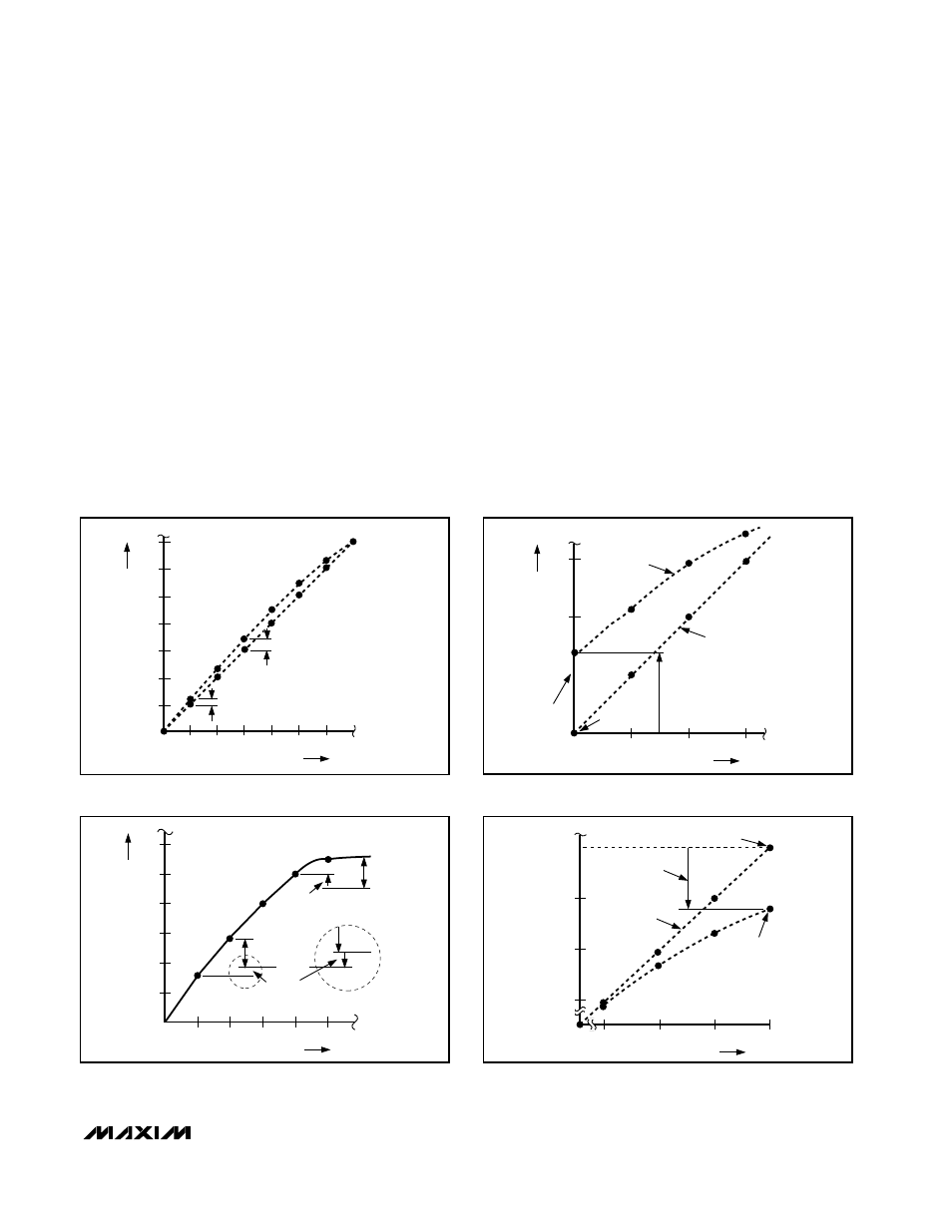
Gain error (Figure 8d) is the difference between the
ideal and the actual full-scale output voltage on the
transfer curve, after nullifying the offset error. This error
alters the slope of the transfer function and corre-
sponds to the same percentage error in each step.
Settling Time
The settling time is the amount of time required from the
start of a transition until the DAC output settles to its new
output value within the converter’s specified accuracy.
Digital Feedthrough
Digital feedthrough is noise generated on the DAC’s
output when any digital input transitions. Proper board
layout and grounding will significantly reduce this
noise, but there will always be some feedthrough
caused by the DAC itself.
Unipolar Output
Figure 9 shows the MAX5132/MAX5133 setup for
unipolar, Rail-to-Rail™ operation with a closed-loop
gain of 2V/V. With its internal reference of +2.5V, the
MAX5132 provides a convenient unipolar output range
of 0 to +4.99939V, while the MAX5133 offers an output
range of 0 to +2.499695V with its on-board +1.25V ref-
erence. Table 5 lists example codes for unipolar output
voltages.
Bipolar Output
The MAX5132/MAX5133 can be configured for unity-
gain bipolar operation (FB = OUT) using the circuit
shown in Figure 10. The output voltage V
OUT
is then
given by the following equation:
V
OUT
= V
REF
[G (NB / 8192) - 1]
0
2
1
4
3
7
6
5
000
010
001
011
100
101
110
AT STEP
011 (1/2 LSB )
AT STEP
001 (1/4 LSB )
111
DIGITAL INPUT CODE
ANALOG OUTPUT VALUE (LSB)
Figure 8a. Integral Nonlinearity
Figure 8b. Differential Nonlinearity
0
2
1
4
3
6
5
000
010
001
011
100
101
DIFFERENTIAL LINEARITY
ERROR (-1/4 LSB)
DIFFERENTIAL
LINEARITY ERROR (+1/4 LSB)
1 LSB
1 LSB
DIGITAL INPUT CODE
ANALOG OUTPUT VALUE (LSB)
0
2
1
3
000
010
001
011
ACTUAL
DIAGRAM
IDEAL DIAGRAM
ACTUAL
OFFSET POINT
OFFSET ERROR
(+1 1/4 LSB)
IDEAL OFFSET
POINT
DIGITAL INPUT CODE
ANALOG OUTPUT VALUE (LSB)
Figure 8c. Offset Error
Figure 8d. Gain Error
0
5
4
6
7
000
101
100
110
111
IDEAL DIAGRAM
GAIN ERROR
(-1 1/4 LSB)
IDEAL FULL-SCALE OUTPUT
ACTUAL
FULL-SCALE
OUTPUT
DIGITAL INPUT CODE
ANALOG OUTPUT VALUE (LSB)
Rail-to-Rail is a registered trademark of Nippon Motorola, Ltd.