Table 2. serial data format, Serial data output, User-programmable output (upo) – Rainbow Electronics MAX5133 User Manual
Page 13

MAX5132/MAX5133
+5V/+3V, 13-Bit, Serial, Force/Sense DACs
with 10ppm/°C Internal Reference
______________________________________________________________________________________
13
PIC16 with SSP Module
and PIC17 Interface
The MAX5132/MAX5133 are compatible with a
PIC16/PIC17 microcontroller (µC), using the synchro-
nous serial port (SSP) module. To establish SPI com-
munication, connect the controller as shown in Figure 4
and configure the PIC16/PIC17 as system master by
initializing its synchronous serial-port control register
(SSPCON) and synchronous serial-port status register
(SSPSTAT) to the bit patterns shown in Tables 3 and 4.
In SPI mode, the PIC16/PIC17 µCs allow eight bits of
data to be synchronously transmitted and received
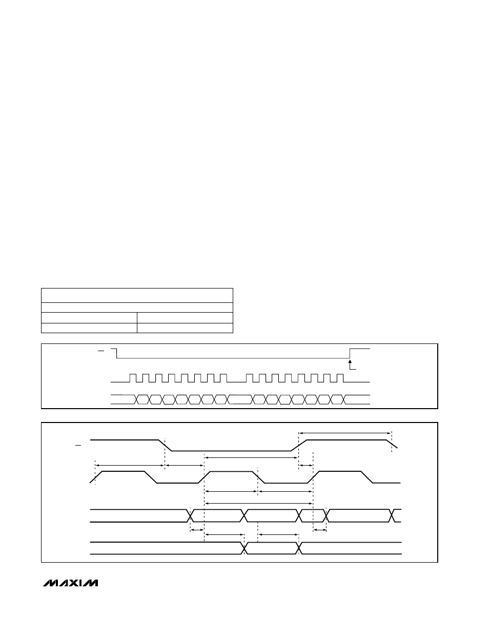
simultaneously. Two consecutive 8-bit writings (Figure
6) are necessary to feed the DAC with three control bits
and 13 data bits. DIN data transitions on the serial
clock’s falling edge and is clocked into the DAC on
SCLK’s rising edge. The first eight bits of DIN contain
the three control bits (C2, C1, C0) and the first five data
bits (D12–D8). The second 8-bit data stream contains
the remaining bits, D7–D0.
Serial Data Output
The contents of the internal shift-register are output seri-
ally on DOUT, which allows for daisy-chaining (see
Applications Information
) of multiple devices as well as
data readback. The MAX5132/MAX5133 may be pro-
grammed to shift data out of DOUT on the serial clock’s
rising edge (Mode 1) or on the falling edge (Mode 0).
The latter is the default during power-up and provides a
lag of 16 clock cycles, maintaining SPI, QSPI,
MICROWIRE, and PIC16/PIC17 compatibility. In Mode
1, the output data lags DIN by 15.5 clock cycles.
During power-down, DOUT retains its last digital state
prior to shutdown.
User-Programmable Output (UPO)
The UPO feature allows an external device to be con-
trolled through the serial-interface setup (Table 1),
thereby reducing the number of microcontroller I/O
ports required. During power-down, this output will
retain the last digital state before shutdown. With CLR
pulled low, UPO will reset to the default state after
wake-up.
CS
SCLK
DIN
COMMAND
EXECUTED
9
8
16
1
C1
C2
D0
C0
D12 D11 D10
D9
D6
D5
D4
D3
D2
D1
D8
D7
Figure 6. Serial-Interface Timing
SCLK
DIN
DOUT
t
CS0
t
CSS
t
CL
t
CH
t
CP
t
CSW
t
CS1
t
CSH
t
DS
t
DO1
t
DO2
t
DH
CS
Figure 7. Detailed Serial-Interface Timing
Table 2. Serial Data Format
C2, C1, C0
D12................................D0
⇐
16 BITS OF SERIAL DATA
⇒
MSB ........................................... LSB
MSB ..... Data Bits ..... LSB
Control Bits
