Definition of terms – Rainbow Electronics MAX9203 User Manual
Page 7
_______________________________________________________________________________________
7
MAX9201/9202/9203
Low Cost, 7ns, Low-Power
Voltage Comparators
Power Supplies
The MAX9201/MAX9202/MAX9203 can be powered
from separate analog and digital supplies or from a sin-
gle +5V supply. The analog supply can range from +5V
to +10V with V
EE
grounded for single-supply operation
(Figures 1a and 1b) or from a split ±5V supply (Figure
1c). The V
DD
digital supply always requires +5V.
In high-speed, mixed-signal applications where a com-
mon ground is shared, a noisy digital environment can
adversely affect the analog input signal. When set up with
separate supplies, the MAX9201/MAX9202/MAX9203
isolate analog and digital signals by providing a separate
analog ground (V
EE
) and digital ground (GND).
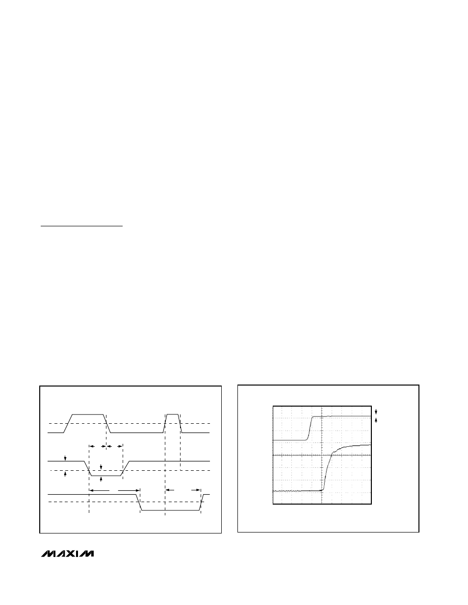
Definition of Terms
V
OS
Input Offset Voltage: Voltage applied be-
tween the two input terminals to obtain TTL
logic threshold (+1.4V) at the output.
V
IN
Input Voltage Pulse Amplitude: Usually set
to 100mV for comparator specifications.
V
OD
Input Voltage Overdrive: Usually set to 5mV
and in opposite polarity to V
IN
for comparator
specifications.
t
pd+
Input to Output High Delay: The propagation
delay measured from the time the input signal
crosses the input offset voltage to the TTL
logic threshold (+1.4V) of an output low to high
transition.
t
pd-
Input to Output Low Delay: The propagation
delay measured from the time the input signal
crosses the input offset voltage to the TTL
logic threshold (+1.4V) of an output high to low
transition.
t
pd+
(D) Latch Disable to Output High Delay: The
propagation delay measured from the latch
signal crossing the TTL logic threshold
(+1.4V) in a low to high transition to the point
of the output crossing TTL threshold (+1.4V)
in a low to high transition.
tpd- (D) Latch Disable to Output Low Delay: The
propagation delay measured from the latch
signal crossing the TTL threshold (+1.4V) in a
low to high transition to the point of the output
crossing TTL threshold (+1.4V) in a high to
low transition.
t
s
Minimum Setup Time: The minimum time,
before the negative transition of the latch sig-
nal, that an input signal change must be pre-
sent in order to be acquired and held at the
outputs.
t
h
Minimum Hold Time: The minimum time,
after the negative transition of the latch sig-
nal, that an input signal must remain
unchanged in order to be acquired and held
at the output.
t
pw
(D) Minimum Latch Disable Pulse Width: The
minimum time that the latch signal must
remain high in order to acquire and hold an
input signal change.
Figure 2. MAX9201/MAX9202/MAX9203 Diagram
Figure 3. t
PD+
Response Time to 5mV Overdrive
LATCH
ENABLE
INPUT
t
pd
t
pd+
(D)
t
pw
(D)
t
s
t
h
V
IN
V
OD
V
OS
LATCH
COMPARE
LATCH
LATCH
COMPARE
COMPARATOR
OUTPUT
1.4V
1.4V
5ns/div
OUTPUT
INPUT
V
OD
+ 5mV
50mV/div
1V/div
0V
0V