Rainbow Electronics MAX9203 User Manual
Page 2
MAX9201/MAX9202/MAX9203
Low Cost, 7ns, Low-Power
Voltage Comparators
2
_______________________________________________________________________________________
ABSOLUTE MAXIMUM RATINGS
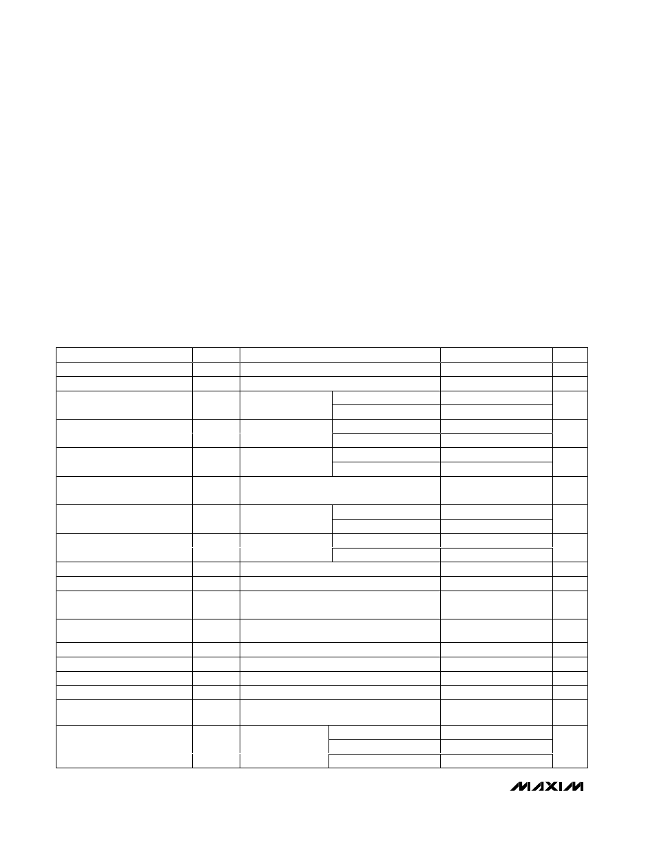
ELECTRICAL CHARACTERISTICS
(V
CC
= +5V, V
EE
= -5V, V
DD
= +5V, GND = 0, V
CM
= 0, LATCH_ = logic high, T
A
= -40
°C to +85°C. Typical values are at T
A
= +25
°C,
unless otherwise noted.) (Note 1)
Stresses beyond those listed under “Absolute Maximum Ratings” may cause permanent damage to the device. These are stress ratings only, and function-
al operation of the device at these or any other conditions beyond those indicated in the operational sections of the specifications is not implied. Exposure
to absolute maximum rating conditions for extended periods may affect device reliability.
Analog Supply Voltage (V
CC
- V
EE
) .....................................+12V
Digital Supply Voltage (V
DD
) .................................................+7V
Differential Input Voltage..................(V
EE
- 0.3V) to (V
CC
+ 0.3V)
Common Mode Input Voltage ..........(V
EE
- 0.3V) to (V
CC
+ 0.3V)
Latch Input Voltage
(MAX9202/MAX9203 only) .....................-0.3V to (V
DD
+ 0.3V)
Output Short-Circuit Duration
To GND ......................................................................Continuous
To V
DD
..................................................................................1min
Continuous Power Dissipation (T
A
= +70°C)
8-Pin SOT23-8 (derate 9.1mW/°C above +70°C) ...727mW/°C
8-Pin SO (derate 5.9mW/°C above +70°C).............471mW/°C
14-Pin TSSOP (derate 9.1mW/°C above +70°C) ....727mW/°C
14-Pin SO (derate 8.3mW/°C above +70°C)...........667mW/°C
16-Pin TSSOP (derate 9.4mW/°C above +70°C) ....755mW/°C
16-Pin SO (derate 8.7mW/°C above +70°C)...........696mW/°C
Operating Temperature Range ...........................-45°C to +85°C
Junction Temperature ......................................................+150°C
Storage Temperature Range ............................-65°C to +150°C
Lead Temperature (soldering, 10s) ................................+300°C
PARAMETER
SYMBOL
CONDITIONS
MIN
TYP
MAX
UNITS
Analog Supply Voltage Range
V
CC
- V
EE
Referenced to V
EE
4.75
10.5
V
Digital Supply Voltage Range
V
DD
Referenced to GND
4.75
5.25
V
T
A
= +25
°C
1
4
Input Offset Voltage
V
OS
V
CM
= 0,
V
OUT
= 1.4V
T
A
= -40
°C to +85°C
7.5
mV
T
A
= +25
°C
1.25
5
Input Bias Current
I
B
I
IN+
or I
IN-
T
A
= -40
°C to +85°C
7.0
µA
T
A
= +25
°C
50
250
Input Offset Current
I
OS
V
CM
= 0,
V
OUT
= 1.4V
T
A
= -40
°C to +85°C
450
nA
Common-Mode Input Voltage
Range
V
CM
Note 2
V
EE
- 0.1
V
C C
-
2.25
V
T
A
= +25
°C
50
150
Common-Mode Rejection
Ratio
CMRR
- 5.1V <
V
C M
< +2.75V
V
OU T
= 1.4V
T
A
= -40
°C to +85°C
250
µV/V
T
A
= +25
°C
50
150
Power-Supply Rejection Ratio
PSRR
Note 3
T
A
= -40
°C to +85°C
250
µV/V
Output High Voltage
V
OH
(V
IN+
- V
IN-
) > 250mV, I
SOURCE
= 1mA
3.0
3.5
V
Output Low Voltage
V
OL
(V
IN+
- V
IN-
) < -250mV, I
SINK
= 8mA
0.25
0.4
V
Latch Input Threshold Voltage
High
V
LH
Note 4
1.4
2
V
Latch Input Threshold Voltage
Low
V
LL
Note 4
0.8
1.4
V
Latch Input Current High
I
LH
V
LH
= 3.0V, Note 4
0.5
3
µA
Latch Input Current Low
I
LL
V
LL
= 0.3V, Note 4
0.5
3
µA
Input Capacitance
C
IN
4
pF
Differential Input Impedance
R
IND
5
M
Ω
Common-Mode Input
Impedance
R
INCM
5.5
M
Ω
MAX9201
4.7
7
MAX9202
2.5
4.0
Positive Analog Supply
Current
I
CC
Note 5
MAX9203
1.3
2
mA