Rainbow Electronics MAX5190 User Manual
Page 13

MAX5187/MAX5190
8-Bit, 40MHz, Current/Voltage-Output DACs
______________________________________________________________________________________
13
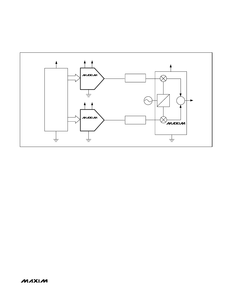
In a typical QAM application (Figure 7), the modulation
occurs in the digital domain, and two DACs such as the
MAX5187/MAX5190 may be used to reconstruct the
analog I and Q components.
The I/Q reconstruction system is completed by a quad-
rature modulator that combines the reconstructed com-
ponents with in-phase and quadrature carrier
frequencies and then sums both outputs to provide the
QAM signal.
Using the MAX5187/MAX5190 for
Arbitrary Waveform Generation
Designing a traditional AWG requires five major func-
tional blocks (Figure 8a): clock generator, counter,
waveform memory, digital-to-analog converter for
waveform reconstruction, and output filter. The wave-
form memory contains a sequentially stored digital
replica of the desired analog waveforms. This memory
shares a common clock with the DAC.
For each clock cycle, a counter adds one count to the
address for the waveform memory. The memory then
loads the next value to the DAC, which generates an
analog output voltage corresponding to that data value
until the next clock cycle. A DAC output filter can either
be a simple or complex lowpass filter, depending on
the AWG requirements for waveform function and fre-
quencies. The main limitations of the AWG’s flexibility
are DAC resolution and dynamic performance, memory
length, clock/playback frequency, and filter character-
istics.
Although the MAX5187/MAX5190 offer high-frequency
operation and excellent dynamics, they are suitable for
relaxed requirements in resolution (8-bit AWGs). To
increase an AWG’s high-frequency accuracy, tempera-
ture stability, wideband tuning, and past phase continu-
ous-frequency switching, the user may approach a
direct digital synthesis (DDS) AWG (Figure 8b). This
DDS loop supports standard waveforms that are repeti-
tive, such as sine, square, TTL, and triangular wave-
forms. DDS allows for precise control of the data
stream input to the DAC. Data for one complete output
waveform cycle is sequentially stored in RAM. As the
RAM addresses change, the DAC converts the incom-
ing data bits into a corresponding voltage waveform.
The resulting output signal frequency is proportional to
the frequency rate at which the RAM addresses are
changed.
Grounding and Power-Supply Decoupling
Grounding and power-supply decoupling strongly influ-
ence the MAX5187/MAX5190’s performance. Unwanted
digital crosstalk may couple through the input, reference,
power-supply, and ground connections, which may
affect dynamic specifications like signal-to-noise ratio or
spurious-free dynamic range. In addition, electromagnet-
BP
FILTER
DV
DD
AV
DD
CARRIER
FREQUENCY
MAX2452
IF
8
Q COMPONENT
MAX5187
MAX5190
BP
FILTER
DV
DD
AV
DD
+3V
8
DIGITAL
SIGNAL
PROCESSOR
QUADRATURE
MODULATOR
I COMPONENT
0
°
90
°
Σ
+3V
MAX5187
MAX5190
Figure 7. Using the MAX5187/MAX5190 for I/Q Signal Reconstruction
