Rainbow Electronics MAX5190 User Manual
Page 12

MAX5187/MAX5190
8-Bit, 40MHz, Current/Voltage-Output DACs
12
______________________________________________________________________________________
Gain Error
Gain error (Figure 5d) is the difference between the
ideal and the actual full-scale output voltage on the
transfer curve, after nullifying the offset error. This error
alters the slope of the transfer function and corre-
sponds to the same percentage error in each step.
Settling Time
Settling time is the amount of time required from the start
of a transition until the DAC output settles its new output
value to within the converter’s specified accuracy.
Digital Feedthrough
Digital feedthrough is the noise generated on a DAC’s
output when any digital input transitions. Proper board
layout and grounding will significantly reduce this
noise, but there will always be some feedthrough
caused by the DAC itself.
Total Harmonic Distortion
Total harmonic distortion (THD) is the ratio of the RMS
sum of the input signal’s first four harmonics to the fun-
damental itself. This is expressed as:
where V
1
is the fundamental amplitude, and V
2
through
V
5
are the amplitudes of the 2nd- through 5th-order
harmonics.
Spurious-Free Dynamic Range
Spurious-free dynamic range (SFDR) is the ratio of RMS
amplitude of the fundamental (maximum signal compo-
nent) to the RMS value of the next-largest distortion com-
ponent.
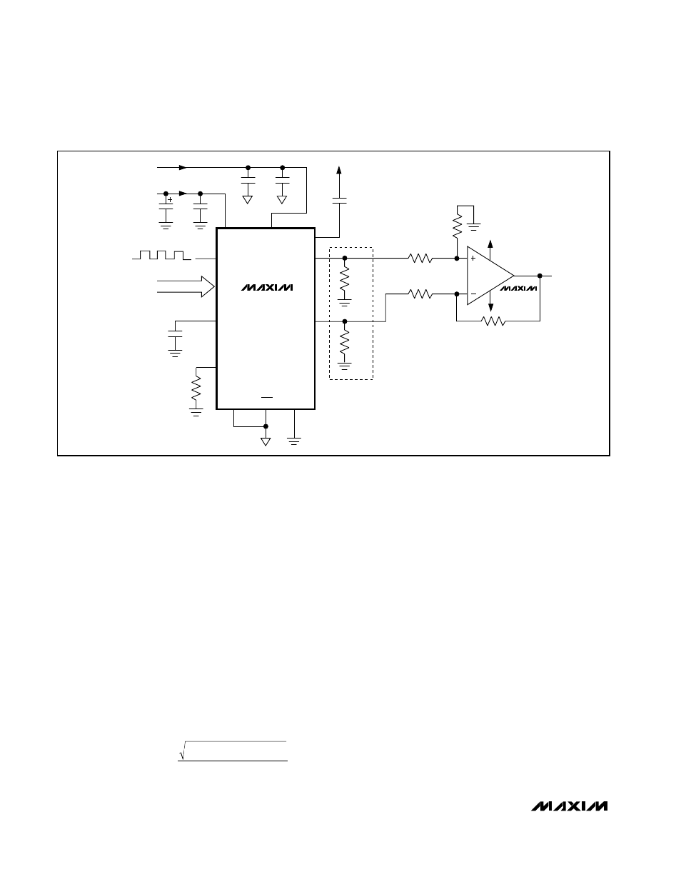
Differential to Single-Ended Conversion
The MAX4108 low-distortion, high-input bandwidth
amplifier may be used to generate a voltage from the
array current output of the MAX5187. The differential
voltage across OUTP and OUTN is converted into a
single-ended voltage by designing an appropriate
operational amplifier configuration (Figure 6).
I/Q Reconstruction in a QAM Application
The low-distortion performance of two MAX5187/
MAX5190s supports analog reconstruction of in-phase
(I) and quadrature (Q) carrier components typically
used in quadrature amplitude modulation (QAM) archi-
tectures, where two separate buses carry the I and Q
data. A QAM signal is both amplitude and phase mod-
ulated, created by summing two independently modu-
lated carriers of identical frequency but different phase
(90° phase difference).
THD
20 log
V
V
V
V
V
2
2
3
2
4
2
5
2
1
=
×
+
+
+
400
Ω*
400
Ω*
REN
AGND
DGND
+5V
-5V
402
Ω
402
Ω
402
Ω
402
Ω
OUTP
CLK
OUTN
0.1
µF
AV
DD
R
SET
**
OUTPUT
MAX5187
MAX5190
10
µF
+3V
+3V
0.1
µF
0.1
µF
REFR
REFO
D0–D7
10
µF
CREF
0.1
µF
AV
DD
DV
DD
MAX4108
*400
Ω RESISTORS INTERNAL TO MAX5190 ONLY.
**MAX5187 ONLY
Figure 6. Differential to Single-Ended Conversion Using a Low-Distortion Amplifier
