Rainbow Electronics MAX5304 User Manual
Page 2
MAX5304
10-Bit Voltage-Output DAC
in 8-Pin µMAX
2
_______________________________________________________________________________________
ABSOLUTE MAXIMUM RATINGS
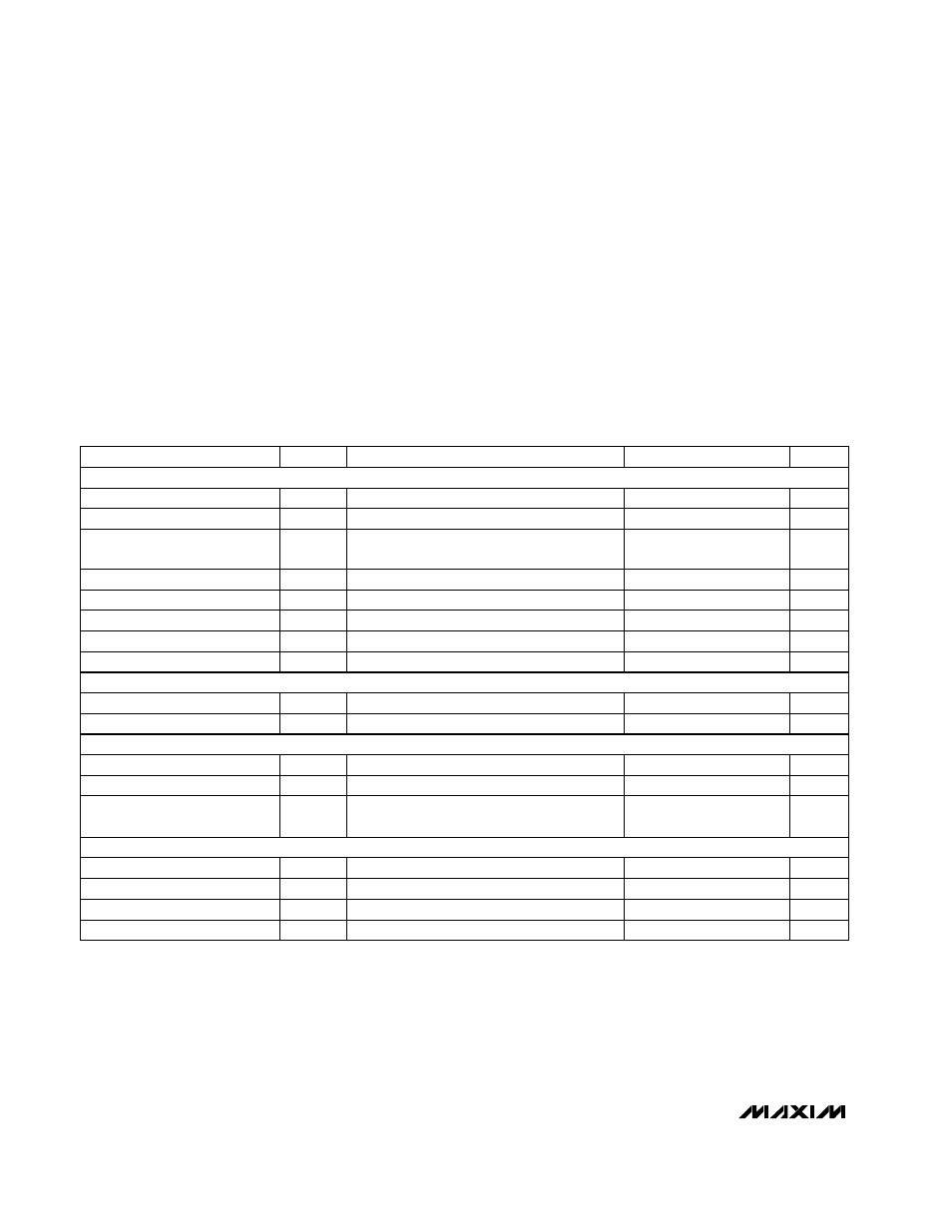
ELECTRICAL CHARACTERISTICS
(Circuit of Figure 8, V
DD
= +5V ±10%, V
REF
= +2.5V, R
L
= 5k
Ω, C
L
= 100pF, T
A
= T
MIN
to T
MAX
, unless otherwise noted. Typical values
are at T
A
= +25°C. Output buffer connected in unity-gain configuration.)
Stresses beyond those listed under “Absolute Maximum Ratings” may cause permanent damage to the device. These are stress ratings only, and functional
operation of the device at these or any other conditions beyond those indicated in the operational sections of the specifications is not implied. Exposure to
absolute maximum rating conditions for extended periods may affect device reliability.
V
DD
to GND...............................................................-0.3V to +6V
REF, OUT, FB to GND.................................-0.3V to (V
DD
+ 0.3V)
Digital Inputs to GND................................................-0.3V to +6V
Continuous Current into Any Pin.......................................±20mA
Continuous Power Dissipation (T
A
= +70°C)
8-Pin µMAX (derate 4.10mW/°C above+70°C) ..........330mW
Operating Temperature Ranges
MAX5304CUA ...................................................0°C to +70°C
MAX5304EUA ................................................-40°C to +85°C
Junction Temperature......................................................+150°C
Storage Temperature Range.............................-65°C to +150°C
Lead Temperature (soldering, 10s)........................... ......+300°C
Code dependent, minimum at code 1550 hex
4.5V
≤ V
DD
≤ 5.5V
Guaranteed monotonic
CONDITIONS
k
Ω
18
30
R
REF
Reference Input Resistance
V
0
V
DD
- 1.4
V
REF
Reference Input Range
µV/V
PSRR
Power-Supply Rejection Ratio
800
Bits
10
N
Resolution
ppm/°C
1
Gain-Error Tempco
LSB
GE
Gain Error (Note 1)
-0.3
±2
ppm/°C
6
TCV
OS
Offset-Error Tempco
LSB
DNL
Differential Nonlinearity
±1.0
±0.3
±8
mV
V
OS
Offset Error
UNITS
MIN
TYP
MAX
SYMBOL
PARAMETER
LSB
±4
INL
Integral Nonlinearity
(Note 1)
V
REF
= 0.67Vp-p
kHz
650
Reference -3dB Bandwidth
Input code = all 0s, V
REF
= 3.6Vp-p at 1kHz
V
REF
= 1Vp-p at 25kHz, code = full scale
dB
77
SINAD
Signal-to-Noise Plus
Distortion Ratio
dB
-84
Reference Feedthrough
V
2.4
V
IH
Input High Voltage
V
IN
= 0 or V
DD
pF
8
C
IN
Input Capacitance
µA
0.001
±0.5
I
IN
Input Leakage Current
V
0.8
V
IL
Input Low Voltage
STATIC PERFORMANCE—ANALOG SECTION
DIGITAL INPUTS
REFERENCE INPUT
MULTIPLYING-MODE PERFORMANCE