Chip information – Rainbow Electronics MAX5304 User Manual
Page 11
MAX5304
10-Bit Voltage-Output DAC
in 8-Pin µMAX
______________________________________________________________________________________
11
Power-Supply Considerations
On power-up, the input and DAC registers are cleared
(set to zero code). For rated MAX5304 performance,
REF must be at least 1.4V below V
DD
. Bypass V
DD
with
a 4.7µF capacitor in parallel with a 0.1µF capacitor to
GND. Use short lead lengths, and place the bypass
capacitors as close to the supply pins as possible.
Grounding and Layout Considerations
Digital or AC transient signals on GND can create noise
at the analog output. Connect GND to the highest-qual-
ity ground available. Good PC board ground layout
minimizes crosstalk between the DAC output, reference
input, and digital input. Reduce crosstalk by keeping
analog lines away from digital lines. Wire-wrapped
boards are not recommended.
DAC
V
OUT
V+
V-
+5V
R1 = R2 = 10k
Ω ±0.1%
MAX5304
REF
R1
R2
FB
OUT
V
DD
GND
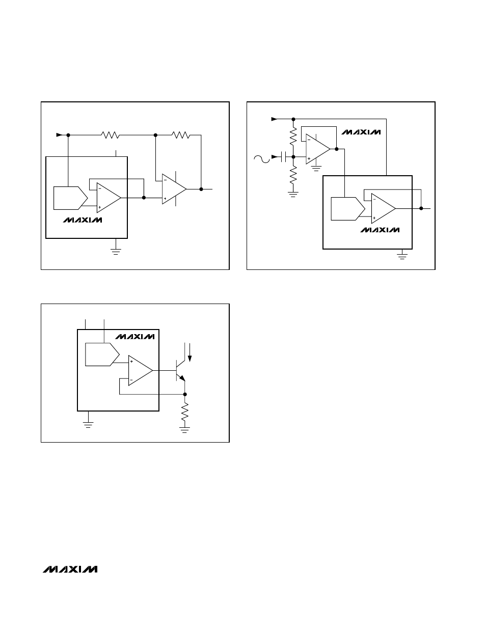
Figure 10. Bipolar Output Circuit
DAC
OUT
MAX5304
10k
26k
REF
V
DD
GND
+5V
+5V
AC
REFERENCE
INPUT
500mVp-p
MAX495
Figure 11. AC Reference Input Circuit
DAC
MAX5304
REF
OUT
R
I
OUT
2N3904
V
L
FB
+5V
V
DD
GND
Figure 12. Digitally Programmable Current Source
___________________Chip Information
TRANSISTOR COUNT: 3053
SUBSTRATE CONNECTED TO AGND