Rainbow Electronics MAX9945 User Manual
Page 2
MAX9945
38V, Low-Noise, MOS-Input,
Low-Power Op Amp
2
_______________________________________________________________________________________
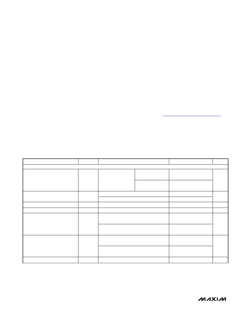
ABSOLUTE MAXIMUM RATINGS
ELECTRICAL CHARACTERISTICS
(V
CC
= +15V, V
EE
= -15V, V
IN+
= V
IN-
= GND = 0, R
OUT
= 100k
Ω to GND, T
A
= -40°C to +125°C, typical values are at T
A
= +25°C,
unless otherwise noted.) (Note 2)
Stresses beyond those listed under “Absolute Maximum Ratings” may cause permanent damage to the device. These are stress ratings only, and functional
operation of the device at these or any other conditions beyond those indicated in the operational sections of the specifications is not implied. Exposure to
absolute maximum rating conditions for extended periods may affect device reliability.
Supply Voltage (V
CC
to V
EE
) ..................................-0.3V to +40V
IN+, IN-, OUT Voltage......................(V
EE
- 0.3V) to (V
CC
+ 0.3V)
IN+ to IN- .............................................................................±12V
OUT Short Circuit to Ground Duration....................................10s
Continuous Input Current into Any Pin .............................±20mA
Continuous Power Dissipation (T
A
= +70°C)
6-Pin TDFN-EP (derate 23.8mW/°C above +70°C)
Multilayer Board ....................................................1904.8mW
Package Thermal Resistance (Note 1)
θ
JA
..............................................................................42°C/W
θ
JC
................................................................................9°C/W
8-Pin µMAX (derate 4.8mW/°C above +70°C)
Multilayer Board ......................................................387.8mW
Package Thermal Resistance (Note 1)
θ
JA
.........................................................................206.3°C/W
θ
JC
..............................................................................42°C/W
Operating Temperature Range .........................-40°C to +125°C
Junction Temperature ......................................................+150°C
Storage Temperature Range .............................-65°C to +150°C
Lead Temperature (soldering, 10s) .................................+300°C
PARAMETER
SYMBOL
CONDITIONS
MIN
TYP
MAX
UNITS
DC ELECTRICAL CHARACTERISTICS
T
A
= +25°C
V
EE
V
CC
-
1.2
Input Voltage Range
V
IN+
, V
IN-
Guaranteed by
CMRR
T
A
= T
MIN
to T
MAX
V
EE
V
CC
-
1.4
V
T
A
= +25°C
±0.6
±5
Input Offset Voltage
V
OS
T
A
= T
MIN
to T
MAX
±8
mV
Input Offset Voltage Drift
V
OS
- T
C
2
µV/°C
Input Bias Current (Note 3)
I
B
50
fA
V
CM
= V
EE
to V
CC
- 1.2V,
T
A
= +25°C
78
94
Common-Mode Rejection Ratio
CMRR
V
CM
= V
EE
to V
CC
- 1.4V,
T
A
= T
MIN
to T
MAX
78
94
dB
V
EE
+ 0.3V
≤ V
OUT
≤ V
CC
- 0.3V,
R
OUT
= 100k
Ω to GND
110
130
Open-Loop Gain
A
OL
V
EE
+ 0.75V
≤ V
OUT
≤ V
CC
- 0.75V,
R
OUT
= 10k
Ω to GND
110
130
dB
Output Short-Circuit Current
I
SC
25
mA
Note 1: Package thermal resistances were obtained using the method described in JEDEC specification JESD51-7, using a four-