Max8727 tft-lcd step-up dc-dc converter, Detailed description – Rainbow Electronics MAX8727 User Manual
Page 7
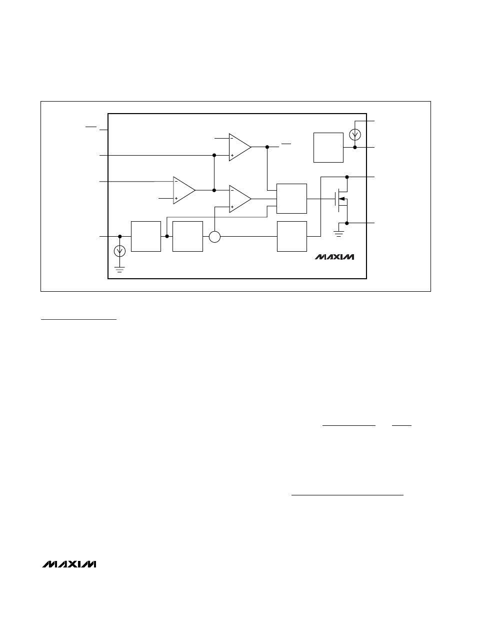
Detailed Description
The MAX8727 is a highly efficient power supply that
employs a current-mode, fixed-frequency, pulse-width
modulation (PWM) architecture for fast transient
response and low-noise operation. The device regu-
lates the output voltage through a combination of an
error amplifier, two comparators, and several signal
generators (Figure 2). The error amplifier compares the
signal at FB to 1.24V and varies the COMP output. The
voltage at COMP determines the current trip point each
time the internal MOSFET turns on. As the load
changes, the error amplifier sources or sinks current to
the COMP output to command the inductor peak cur-
rent necessary to service the load. To maintain stability
at high duty cycles, a slope-compensation signal is
summed with the current-sense signal.
At light loads, this architecture allows the MAX8727 to
“skip” cycles to prevent overcharging the output voltage.
In this region of operation, the inductor ramps up to a
peak value of approximately 50mA, discharges to the
output, and waits until another pulse is needed again.
Output Current Capability
The output current capability of the MAX8727 is a func-
tion of current limit, input voltage, operating frequency,
and inductor value. Because of the slope compensa-
tion used to stabilize the feedback loop, the inductor
current limit depends on the duty cycle. The current
limit is determined by the following equation:
I
LIM
= (1.26 - 0.35 x D) x I
LIM_EC
where I
LIM
_
EC
is the current limit specified at 75% duty
cycle (see the Electrical Characteristics) and D is the
duty cycle.
The output current capability depends on the current-
limit value and is governed by the following equation:
where I
LIM
is the current limit calculated above,
η is the
regulator efficiency (85% nominal), and D is the duty
cycle. The duty cycle when operating at the current
limit is:
where V
DIODE
is the rectifier diode forward voltage and
R
ON
is the on-resistance of the internal MOSFET.
D
V
V
V
V
I
R
V
OUT
IN
DIODE
OUT
LIM
ON
DIODE
=
−
+
−
×
+
I
I
D
V
f
L
V
V
OUT MAX
LIM
IN
OSC
IN
OUT
(
)
.
=
−
Ч
Ч
Ч
⎡
⎣
⎢
⎢
⎤
⎦
⎥
⎥
Ч
Ч
0 5
η
MAX8727
TFT-LCD Step-Up DC-DC Converter
_______________________________________________________________________________________
7
GND
LX
IN
FREQ
FB
COMP
4
µA
5
µA
N
ERROR
COMPARATOR
ERROR
AMPLIFIER
SKIP
COMPARATOR
SS
CLOCK
SKIP
BIAS
SHDN
MAX8727
Σ
CURRENT
SENSE
CONTROL
AND DRIVER
LOGIC
SOFT-
START
SLOPE
COMPEN-
SATION
OSCILLATOR
∞
1.24V
Figure 2. MAX8727 Functional Diagram