Electrical characteristics (continued) – Rainbow Electronics MAX9730 User Manual
Page 3
MAX9730
2.4W, Single-Supply, Class G Power Amplifier
_______________________________________________________________________________________
3
ELECTRICAL CHARACTERISTICS (continued)
(V
CC
= CPV
DD
= SHDN = 3.6V, GND = CPGND = 0V, R
IN+
= R
IN-
= 10kΩ, R
FB+
= R
FB-
= 10kΩ, R
FS
= 100kΩ, C1 = 4.7µF, C2 =
10µF; speaker load resistors (R
L
) are terminated between OUT+ and OUT-, unless otherwise stated; T
A
= T
MIN
to T
MAX
, unless other-
wise noted. Typical values are at T
A
= +25°C.) (Notes 1, 2)
Note 1:
All devices are 100% production tested at room temperature. All temperature limits are guaranteed by design.
Note 2:
Testing performed with resistive and inductive loads to simulate an actual speaker load. For dynamic speakers,
R
L
= 8Ω, 68µH.
Note 3:
Designed for 1.8V logic.
Note 4:
R
IN_
and R
FB_
have 0.5% tolerance.
Note 5:
Amplifier inputs AC-coupled to GND.
Note 6:
Testing performed at room temperature with 8Ω resistive load in series with 68µH inductive load connected across BTL
output for speaker amplifier. Mode transitions are controlled by SHDN. V
CP
is the peak output transient expressed in dBV.
Note 7:
Voltage gain is defined as: [V
OUT+
- V
OUT-
] / [V
IN+
- V
IN-
].
Note 8:
Mode A tone burst tested at full amplitude for one cycle and half amplitude for nine cycles. Mode B tone burst tested at
full amplitude for three cycles and half amplitude for seven cycles. Full amplitude is defined as 1% THD+N at full battery
(V
CC
= 4.2V).
Electrical Characteristics table targets must be met at THD+N = 1% for one cycle (Mode A) and THD+N <
5% for three cycles (Mode B).
Note 9:
Dynamic range is calculated by measuring the RMS voltage difference between a -60dBFS output signal and the noise
floor, then adding 60dB. Full scale is defined as the output signal needed to achieve 1% THD+N.
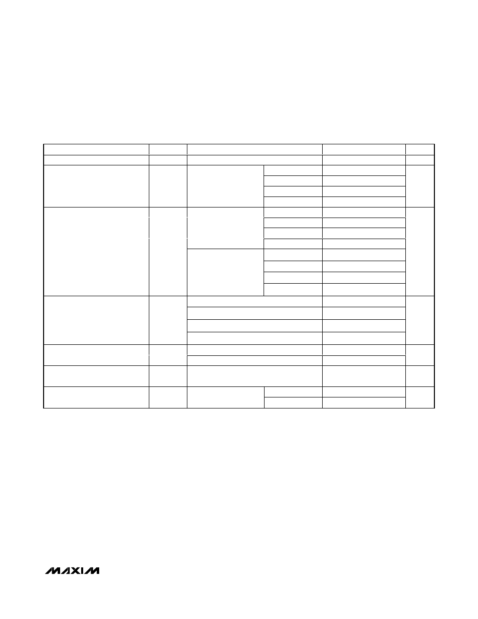
PARAMETER
SYMBOL
CONDITIONS
MIN
TYP
MAX
UNITS
Voltage Gain
A
V
(Notes 4, 7)
11.5
12
12.5
dB
V
CC
= 5V
2.4
V
CC
= 4.2V
1.67
V
CC
= 3.6V
1.25
Continuous Output Power
P
OUT
THD+N = 1%, f = 1kHz,
R
L
= 8
Ω
V
CC
= 3.0V
0.8
V
RMS
V
CC
= 5V
7.1
V
CC
= 4.2V
5.9
V
CC
= 3.6V
5.1
f = 1kHz, 1% THD+N,
Z
L
= 1µF + 10
Ω
V
CC
= 3.0V
4.2
V
CC
= 5V
6.5
V
CC
= 4.2V
5.4
V
CC
= 3.6V
4.7
Output Voltage
V
OUT
f = 10kHz, 1% THD+N,
Z
L
= 1µF + 10
Ω, no
load
V
CC
= 3.0V
3.8
W
V
CC
= 2.7V to 5.5V
63
77
f = 217Hz, 200mV
P-P
ripple
77
f = 1kHz, 200mV
P-P
ripple
77
Power-Supply Rejection Ratio
(Note 4)
PSRR
f = 20kHz, 200mV
P-P
ripple
58
dB
R
L
= 8
Ω, V
OUT
= 1kHz / 400mW
0.007
Total Harmonic Distortion Plus
Noise
THD+N
R
L
= 8
Ω, V
OUT
= 1kHz / 1W
0.12
%
Signal-to-Noise Ratio
SNR
V
OUT
= 0.5W, inputs to GND by C1N,
A-weighted
95
dB
22Hz to 22kHz
96
Dynamic Range
DR
(Note 9)
A-weighted
99
dB