Max9730, 4w, single-supply, class g power amplifier, Ucsp applications information – Rainbow Electronics MAX9730 User Manual
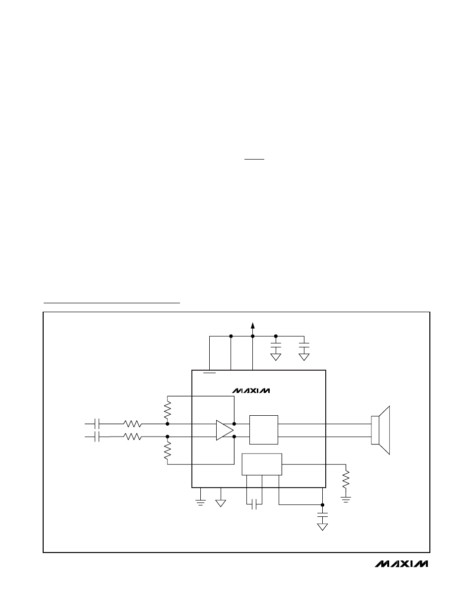
Page 10: Typical application circuit/functional diagram, Thermal considerations
MAX9730
Thermal Considerations
Class G amplifiers provide much better efficiency and
thermal performance than a comparable Class AB
amplifier. However, the system’s thermal performance
must be considered with realistic expectations and
include consideration of many parameters. This section
examines Class G amplifiers using general examples to
illustrate good design practices.
TQFN Considerations
The exposed pad is the primary route of keeping heat
away from the IC. With a bottom-side exposed pad, the
PCB and its copper become the primary heatsink for
the Class G amplifier. Solder the exposed pad to a
large copper polygon that is connected to the ground
plane.
The copper polygon to which the exposed pad is
attached should have multiple vias to the opposite side
of the PCB, where they connect to GND. Make this
polygon as large as possible within the system’s con-
straints.
UCSP Applications Information
For the latest application details on UCSP construction,
dimensions, tape carrier information, PCB techniques,
bump-pad layout, and recommended reflow tempera-
ture profile, as well as the latest information on reliability
testing results, go to the Maxim website at www.maxim-
ic.com/ucsp for the application note,
UCSP—A Wafer-
Level Chip-Scale Package
.
2.4W, Single-Supply, Class G Power Amplifier
10
______________________________________________________________________________________
Typical Application Circuit/Functional Diagram
MAX9730
+
IN+
FB+
1 (B2)
0.1
μF
4 (A3)
14, 22
(D1, D5)
R
IN-
10k
Ω
V
CC
R
IN-
10k
Ω
C
IN
1
μF
C
IN
1
μF
IN-
20 (D2)
16 (D4)
FB-
OUT+
13 (C5)
( ) UCSP PACKAGE
DEVICE SHOWN WITH A
V
= 12dB
*SYSTEM-LEVEL REQUIREMENT TYPICALLY 10
μF
FS
OUT-
10 (B5)
7 (A4)
9 (A5)
12 (B4)
18 (D3)
27 (A1)
26 (B1)
3 (A2) 24 (C1)
15, 21
(C2, C4)
-
CLASS G
OUTPUT
STAGE
CHARGE
PUMP
R
FB+
10k
Ω
R
FB-
10k
Ω
SHDN
CPGND
PV
SS
SV
SS
C1N
C1P
C2
10
μF
R
FS
100k
Ω
GND
CPV
DD
C1
4.7
μF
V
DD
*