Rainbow Electronics MAX6869 User Manual
Page 2
MAX6854–MAX6869
Nanopower µP Supervisory Circuits with
Optional Manual Reset, Watchdog Timer
2
_______________________________________________________________________________________
ABSOLUTE MAXIMUM RATINGS
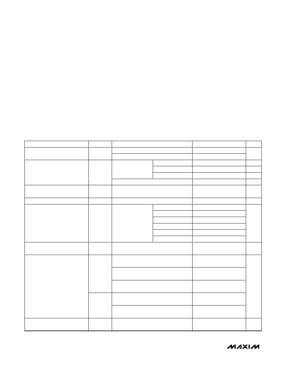
ELECTRICAL CHARACTERISTICS
(V
CC
= 1.2V to 5.5V, T
A
= -40°C to +85°C, unless otherwise specified. Typical values are at V
CC
= 2.5V, T
A
= +25°C.) (Note 1)
Stresses beyond those listed under “Absolute Maximum Ratings” may cause permanent damage to the device. These are stress ratings only, and functional
operation of the device at these or any other conditions beyond those indicated in the operational sections of the specifications is not implied. Exposure to
absolute maximum rating conditions for extended periods may affect device reliability.
V
CC
, Open-Drain RESET to GND ..........................-0.3V to +6.0V
MR, Push-Pull RESET, RESET,
WDI, CT, I.C............................................-0.3V to (V
CC
+ 0.3V)
Input Current, Output Current (all pins)............................±20mA
Continuous Power Dissipation (T
A
= +70°C)
5-Pin SOT23 (derate 7.1mW/°C above +70°C)............571mW
Operating Temperature Range ...........................-40°C to +85°C
Junction Temperature .....................................................+150°C
Storage Temperature Range .............................-65°C to +150°C
Lead Temperature (soldering, 10s) .................................+300°C
PARAMETER
SYMBOL
CONDITIONS
MIN
TYP
MAX
UNITS
T
A
≥
0°C
1.1
5.5
Supply Voltage
V
CC
T
A
= -40°C to +85°C
1.2
5.5
V
V
CC
= 5.0V
210
400
nA
V
CC
= 3.3V
190
380
nA
V
CC
> V
TH
, no load,
reset output
deasserted (Note 2)
V
CC
= 1.8V
170
370
nA
Supply Current
I
CC
V
CC
< V
TH
, no load, reset output asserted
7
15
µA
V
CC
Reset Threshold
V
TH
V
CC
falling (see Table 2)
V
TH
-
2.5%
V
TH
V
TH
+
2.5%
V
Reset Threshold Hysteresis
V
HYST
Reset asserted to reset deasserted
0.5
%V
TH
D1
10
15
25
D2
40
60
80
D3
150
225
300
D4
1200
1800
2400
D5
300
450
600
Reset Timeout Period
t
RP
V
CC
= V
TH
+ 150mV
(Figures 2 and 3)
D6
600
900
1200
ms
V
CC
to Reset Delay
t
RD
V
CC
falling from (V
TH
+ 100mV) to
(V
TH
- 100mV) at 10mV/µs
40
µs
V
CC
≥
1.1V, I
SINK
= 50µA,
RESET asserted, T
A
≥
0°C
0.3
V
CC
≥
1.2V, I
SINK
= 100µA,
RESET asserted
0.3
V
OL
V
CC
≥
2.12V, I
SINK
= 1.2mA,
RESET asserted
0.3
V
CC
≥
1.71V, I
SOURCE
= 200µA,
RESET deasserted, push-pull RESET only
0.8 x V
CC
RESET Output Voltage
V
OH
V
CC
≥
2.38V, I
SOURCE
= 500µA,
RESET deasserted, push-pull RESET only
0.8 x V
CC
V
Open-Drain RESET Leakage
Current
I
LKG
RESET deasserted
25
nA