Electrical characteristics—max5150 (continued) – Rainbow Electronics MAX5151 User Manual
Page 3
MAX5150/MAX5151
Low-Power, Dual, 13-Bit Voltage-Output DACs
with Serial Interface
_______________________________________________________________________________________
3
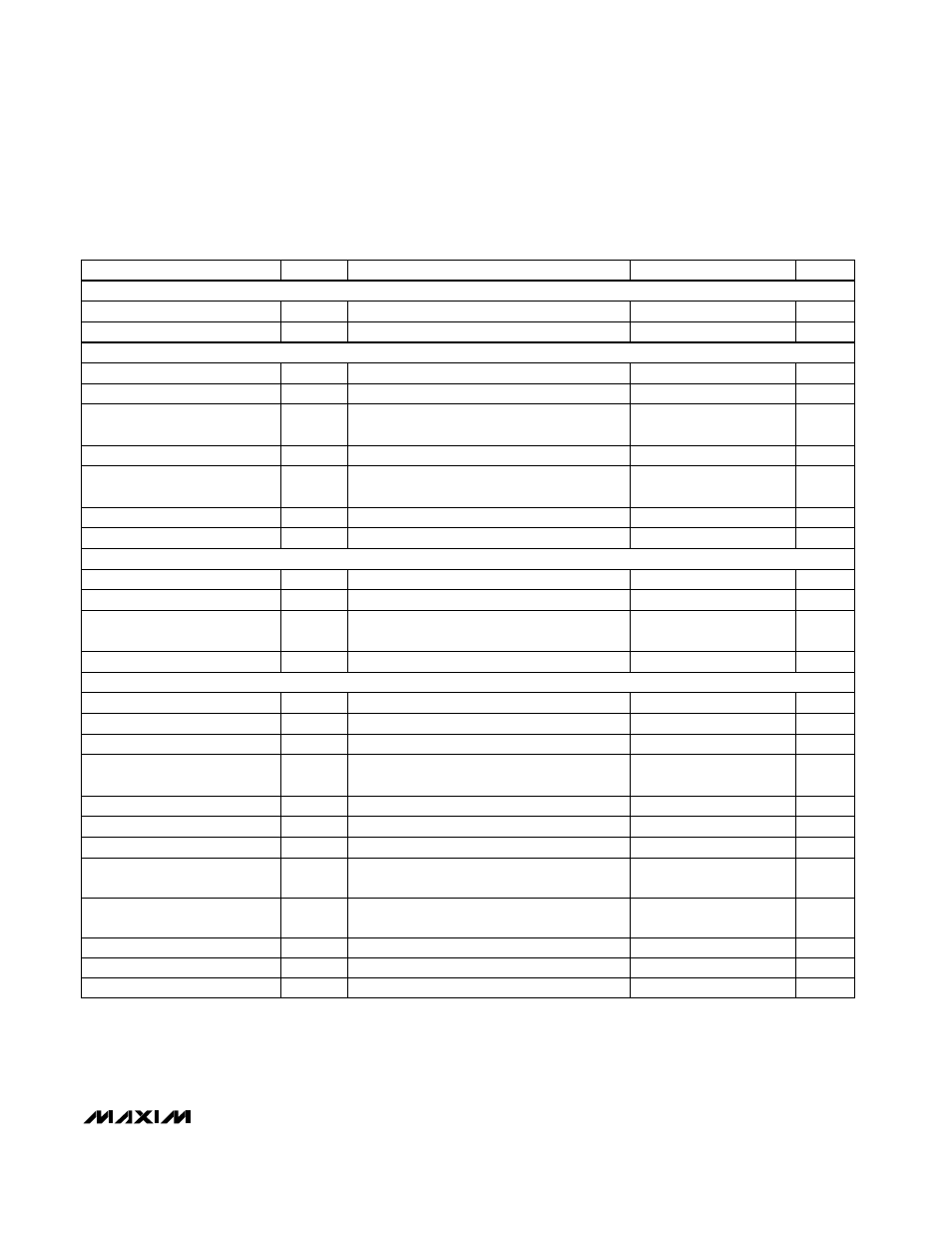
ELECTRICAL CHARACTERISTICS—MAX5150 (continued)
(V
DD
= +5V ±10%, V
REFA
= V
REFB
= 2.048V, R
L
= 10k
Ω
, C
L
= 100pF, T
A
= T
MIN
to T
MAX
, unless otherwise noted. Typical values are
at T
A
= +25°C (OS_ tied to AGND for a gain of +2).)
CONDITIONS
Rail-to-rail (Note 2)
To 1/2LSB of full-scale, V
STEP
= 4V
I
SOURCE
= 2mA
UNITS
I
SINK
= 2mA
k
Ω
24
34
R
OS
OSA or OSB Input Resistance
V
0 to V
DD
Output Voltage Swing
µs
16
Output Settling Time
V/µs
0.75
SR
Voltage Output Slew Rate
V
OL
Output Low Voltage
V
0.13
0.4
MIN
TYP
MAX
SYMBOL
PARAMETER
V
OH
Output High Voltage
V
V
DD -
0.5
µs
25
Time Required to Exit Shutdown
CS = V
DD
, f
DIN
= 100kHz, V
SCLK
= 5Vp-p
nV-s
5
Digital Feedthrough
nV-s
5
Digital Crosstalk
V
4.5
5.5
V
DD
Positive Supply Voltage
(Note 3)
mA
0.5
0.65
I
DD
Power-Supply Current
(Note 3)
µA
2
10
I
DD (SHDN)
Power-Supply Current
in Shutdown
µA
0
±1
Reference Current in Shutdown
ns
100
t
CP
SCLK Clock Period
ns
40
t
CH
SCLK Pulse Width High
ns
40
t
CL
SCLK Pulse Width Low
ns
40
t
CSS
CS Fall to SCLK Rise
Setup Time
ns
0
t
CSH
SCLK Rise to CS Rise Hold Time
ns
40
t
DS
SDI Setup Time
ns
0
t
DH
SDI Hold Time
C
LOAD
= 200pF
ns
80
t
DO1
SCLK Rise to DOUT
Valid Propagation Delay
Note 1:
Accuracy is specified from code 12 to code 8191.
Note 2:
Accuracy is better than 1LSB for V
OUT
_ greater than 6mV and less than V
DD
- 50mV. Guaranteed by PSRR test at the end
points.
Note 3:
Digital inputs are set to either V
DD
or DGND, code = 0000 hex, R
L
=
∞
.
C
LOAD
= 200pF
ns
80
t
DO2
SCLK Fall to DOUT
Valid Propagation Delay
ns
40
t
CS1
CS Rise to SCLK Rise Hold
ns
100
t
CSW
CS Pulse Width High
ns
10
t
CS0
SCLK Rise to CS Fall Delay
DYNAMIC PERFORMANCE
POWER SUPPLIES
DIGITAL OUTPUTS
TIMING CHARACTERISTICS