Rainbow Electronics MAX5151 User Manual
Page 15
The microprocessor then programs the DAC to set an
output voltage at the midpoint of the two calibrated val-
ues. Applications include tachometers, motion sensing,
automatic readers, and liquid clarity analysis.
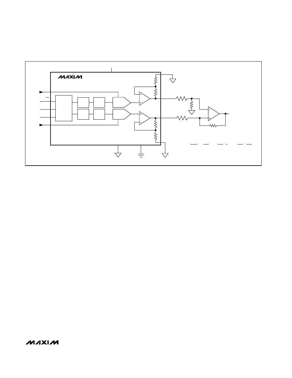
Digital Control of Gain and Offset
The two DACs can be used to control the offset and
gain for curve-fitting nonlinear functions, such as trans-
ducer linearization or analog compression/expansion
applications. The input signal is used as the reference
for the gain-adjust DAC, whose output is summed with
the output from the offset-adjust DAC. The relative
weight of each DAC output is adjusted by R1, R2, R3,
and R4 (Figure 14).
Power-Supply Considerations
On power-up, the input and DAC registers clear (set to
zero code). For rated performance, V
REF_
should be at
least 1.4V below V
DD
. Bypass the power supply with a
4.7µF capacitor in parallel with a 0.1µF capacitor to
AGND. Minimize lead lengths to reduce lead induc-
tance.
Grounding and Layout Considerations
Digital and AC transient signals on AGND can create
noise at the output. Connect AGND to the highest quali-
ty ground available. Use proper grounding techniques,
such as a multilayer board with a low-inductance
ground plane. Carefully lay out the traces between
channels to reduce AC cross-coupling and crosstalk.
Wire-wrapped boards and sockets are not recommend-
ed. If noise becomes an issue, shielding may be
required.
MAX5150/MAX5151
Low-Power, Dual, 13-Bit Voltage-Output DACs
with Serial Interface
______________________________________________________________________________________
15
AGND
DGND
MAX5150
MAX5151
DACA
V
DD
REFA
V
IN
V
REF
CS
SCLK
DIN
REFB
R1
R3
R
R
R
R
R4
R2
OUTB
OSB
OUTA
OSA
V
OUT
DACB
INPUT
REG A
INPUT
REG B
DAC
REG A
DAC
REG B
– OFFSET
[ ]
V
OUT
=
=
GAIN
[ ]
2NA
8192
NA IS THE NUMERIC VALUE OF THE INPUT CODE FOR DACA.
NB IS THE NUMERIC VALUE OF THE INPUT CODE FOR DACB.
R2
R1+R2
R4
R3
2NB
8192
R4
R3
(
V
IN
)(
)(
1+
) (
V
REF
)( )
[ ] [ ]
SHIFT
REGISTER
Figure 14. Digital Control of Gain and Offset