Vishay high power products, Half-bridge" igbt mtp (warp speed igbt), 114 a, Electrical specifications (t – C&H Technology 50MT060WHTAPbF User Manual
Page 3: 25 °c unless otherwise specified), Switching characteristics (t
www.vishay.com
For technical questions, contact: [email protected]
Document Number: 94468
2
Revision: 06-May-08
50MT060WHTAPbF
Vishay High Power Products
"Half-Bridge" IGBT MTP
(Warp Speed IGBT), 114 A
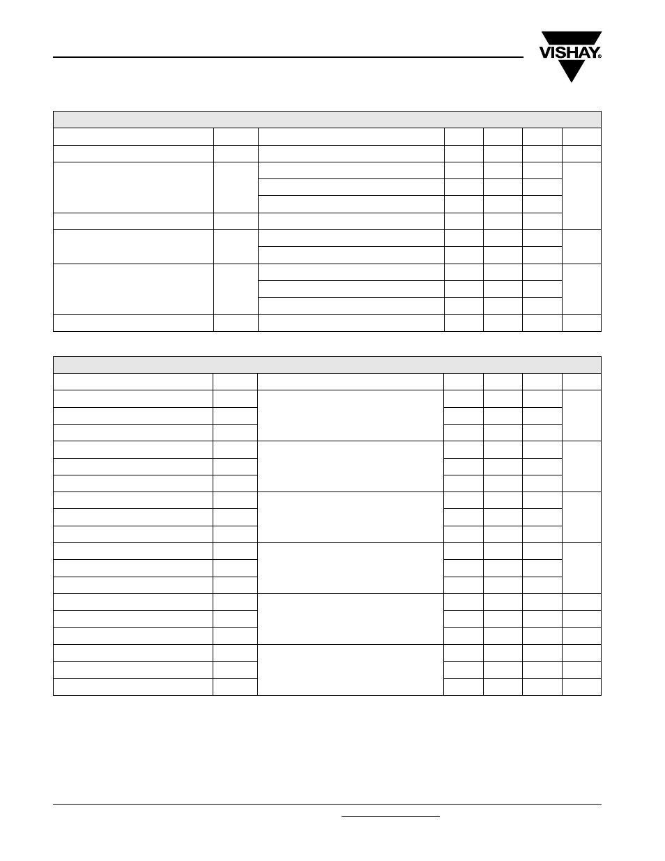
ELECTRICAL SPECIFICATIONS (T
J
= 25 °C unless otherwise specified)
PARAMETER SYMBOL
TEST
CONDITIONS
MIN.
TYP.
MAX.
UNITS
Collector to emitter breakdown voltage
V
(BR)CES
V
GE
= 0 V, I
C
= 500 µA
600
-
-
V
Collector to emitter voltage
V
CE(on)
V
GE
= 15 V, I
C
= 50 A
-
2.3
3.15
V
V
GE
= 15 V, I
C
= 100 A
-
2.5
3.2
V
GE
= 15 V, I
C
= 50 A, T
J
= 150 °C
-
1.72
2.17
Gate threshold voltage
V
GE(th)
I
C
= 0.5 mA
3
-
6
Collector to emitter leaking current
I
CES
V
GE
= 0 V, I
C
= 600 A
-
-
0.4
mA
V
GE
= 0 V, I
C
= 600 A, T
J
= 150 °C
-
-
10
Diode forward voltage drop
V
FM
I
F
= 50 A, V
GE
= 0 V
-
1.58
1.80
V
I
F
= 50 A, V
GE
= 0 V, T
J
= 150 °C
-
1.49
1.68
I
F
= 100 A, V
GE
= 0 V, T
J
= 25 °C
-
1.9
2.17
Gate to emitter leakage current
I
GES
V
GE
= ± 20 V
-
-
± 250
nA
SWITCHING CHARACTERISTICS (T
J
= 25 °C unless otherwise specified)
PARAMETER SYMBOL
TEST
CONDITIONS
MIN.
TYP.
MAX.
UNITS
Total gate charge (turn-on)
Q
g
I
C
= 52 A
V
CC
= 400 V
V
GE
= 15 V
-
331
385
nC
Gate to emitter charge (turn-on)
Q
ge
-
44
52
Gate to collector charge (turn-on)
Q
gc
-
133
176
Turn-on switching loss
E
on
Internal gate resistors (see electrical diagram)
I
C
= 50 A, V
CC
= 480 V, V
GE
= 15 V, L = 200 µH
Energy losses include tail and diode reverse
recovery
-
0.26
-
mJ
Turn-off switching loss
E
off
-
1.2
-
Total switching loss
E
ts
-
1.46
-
Turn-on switching loss
E
on
Internal gate resistors (see electrical diagram)
I
C
= 50 A, V
CC
= 480 V, V
GE
= 15 V, L = 200 µH
Energy losses include tail and diode reverse
recovery, T
J
= 150 °C
-
0.73
-
mJ
Turn-off switching loss
E
off
-
1.66
-
Total switching loss
E
ts
-
2.39
-
Input capacitance
C
ies
V
GE
= 0 V
V
CC
= 30 V
f = 1.0 mHz
-
7100
-
pF
Output capacitance
C
oes
-
510
-
Reverse transfer capacitance
C
res
-
140
-
Diode reverse recovery time
t
rr
V
CC
= 200 V, I
C
= 50 A
dI/dt = 200 A/µs
-
82
97
ns
Diode peak reverse current
I
rr
-
8.3
10.6
A
Diode recovery charge
Q
rr
-
340
514
nC
Diode reverse recovery time
t
rr
V
CC
= 200 V, I
C
= 50 A
dI/dt = 200 A/µs
T
J
= 125 °C
-
137
153
ns
Diode peak reverse current
I
rr
-
12.7
14.8
A
Diode recovery charge
Q
rr
-
870
1132
nC